Posts | Comments

Planet Arduino

Archive for the ‘pcb’ Category

Jul
01

48 Solenoids Transform This 1960s Typewriter into a Computer Printer

arduino, Computers & Mobile, Corona, Midi, pcb, Retro, solenoid, Tufts, typewriter, vintage Comments Off on 48 Solenoids Transform This 1960s Typewriter into a Computer Printer 

typewriter-solenoidsSeveral years ago, Chris Gregg, a Tufts University lecturer and computer engineer, received a letter from his friend Erica. This wouldn’t be so unusual, except that it was typed on an actual typewriter, not a printer. Gregg is a fan of vintage typewriters, but, as with myself, makes many mistakes, […]

Read more on MAKE

The post 48 Solenoids Transform This 1960s Typewriter into a Computer Printer appeared first on Make: DIY Projects, How-Tos, Electronics, Crafts and Ideas for Makers.

May
04

Design Your Own PCB Business Card

arduino, business card, pcb Comments Off on Design Your Own PCB Business Card 

FBFGL8QI93F6Y3B.MEDIUM

by Proto G @ instructables.com:

In this instructable I am going to show you how to make your own printed circuit board business card. I feel that these business cards will really help you stand out from the crowd and make a great impression. It might even add one more skill to your resume. Everyone that I have given these cards out to has been really impressed and thought it was a great idea. I have regular business cards as well and I only selectively give out my circuit board cards. You can take it to the next level by soldering different circuits on the cards. I made one of my cards into a standalone Arduino.

Design Your Own PCB Business Card – [Link]

Jul
28

Fritzing is out with a new release including Arduino Yún microcontroller!

circuit, education, Featured, Fritzing, new release, pcb, Software Comments Off on Fritzing is out with a new release including Arduino Yún microcontroller! 

Fritzing is an open-source hardware initiative that makes electronics accessible as a creative material for anyone. You can easily learn how to build a circuit for you project and also design your own PCB.

Last week, the Fritzing team announced the new release with a number of new parts, especially a number of popular microcontrollers, among which also Arduino Yún:

We have upgraded to their latest version Qt5, which brings stability and speed improvements (especially for Mac OS X users). This also enables us to port fritzing to Android, iOS, etc.

You can download Fritzing 0.9.0b at this link.


Jun
23

Handheld Game System Powered by Arduino

adafruit, arduino, arduino hacks, ATmega, Gaming, LCD, pcb, portable, Shapeoko, Video Games Comments Off on Handheld Game System Powered by Arduino 

DIY Handheld Game System

These days, it’s easy enough to play games on the go. If you have a smart phone, you are pretty much set. That doesn’t mean you can’t still have fun designing and building your own portable gaming system, though.

[randrews] did just that. He started out by purchasing a small memory LCD display from Adafruit. The screen he chose is low power as far as screens go, so it would be a good fit for this project. After testing the screen with a quick demo program, it was time to start designing the circuit board.

[randrews] used Eagle to design the circuit. He hand routed all of the traces to avoid any weird issues that the auto router can sometimes cause. He made an efficient use of the space on the board by mounting the screen over top of the ATMega chip and the other supporting components. The screen is designed to plug in and out of the socket, this way it can be removed to get to the chip. [randrews] needs to be able to reach the chip in order to reprogram it for different games.

Once the board design was finished, [randrews] used his Shapeoko CNC mill to cut it out of a copper clad board. He warns that you need to be careful doing this, since breathing fiberglass dust is detrimental to living a long and healthy life. Once the board was milled out, [randrews] used a small Dremel drill press to drill all of the holes.

The final piece of the puzzle was to figure out the power situation. [randrews] designed a second smaller PCB for this. The power board holds two 3V coin cell batteries. The Arduino expects 5V, so [randrews] had to use a voltage regulator. This power board also contains the power switch for the whole system.

The power board was milled and populated. Then it was time to do some measurements. [randrews] measured the current draw and calculates that he should be able to get around 15 hours of play time using the two 3V coin cell batteries. Not bad considering the size.

[via Reddit]


Filed under: Arduino Hacks
Mar
01

The Credit Card Sized GameBoy

Arduboy, arduino hacks, Hardware, pcb, PCB milling Comments Off on The Credit Card Sized GameBoy 

arduboy

Think you’ve seen every possible type of Arduino based hand held video game? [Kevin] managed to coax something new out of the theme with a very clever credit card sized console that uses some very interesting construction techniques.

The inspiration for this project began when [Kevin] dropped an SMD resistor into a drill hole on a PCB. This resistor fell right through the hole, giving him the idea creating a PCB with milled cutouts made to fit SMD components. With a little experimentation, [Kevin] found he could fit a TQFP32 ATMega328p  - the same microcontroller in the Arduino – in a custom square cutout. The rest of the components including a CR2016 battery and OLED display use the same trick.

The rest of the design involved taking Adafruit and Sparkfun breakout boards, and modifying the individual circuits until something broke. Then, off to Eagle to create a PCB.

[Kevin]‘s experiment in extremely unusual PCB design worked, resulting in a credit-card sized “Game Boy” that’s only 1.6 millimeters thick. The controls are capacitive touch sensors and he already has an easter egg hidden in the code; enter the Konami code and the Hackaday logo pops up to the tune of [Rick Astley]‘s magnum opus.

Now [Kevin] is in a bit of a bind. He’d like to take this prototype and turn it into a crowd sourced campaign. In our opinion, this “Game Boy in a wallet” would probably do well on a site like Tindie, but any sort of large scale manufacturing is going to be a rather large pain. If you have any wishes, advice, of complaints for [Kevin] he’s got a few links at the bottom of his project page.


Filed under: Arduino Hacks, hardware
Jan
09

New Project: Make Your Own D*mn Board – Part 2: Routing

arduino, Eagle, Electronics, layout, modern device, pcb, RBBB, Software, tutorial Comments Off on New Project: Make Your Own D*mn Board – Part 2: Routing 

M36_089_SkillBld_F1We're learning how to use EAGLE by stepping through the design process for a basic Arduino-type AVR microcontroller development board, specifically the Really Bare Bones Board design by Paul Badger of Modern Device. In Part 1, we showed you how to lay out the schematic and validate it with EAGLE's built-in Electrical Rule Check. Here we'll show you how to establish the physical shape of the board and the actual copper pathways that make up the real circuit.

Read more on MAKE

Oct
29

New Project: Make Your Own D*mn Board – Part 3: Silkscreen and Gerbers

arduino, Eagle, Electronics, layout, modern device, pcb, RBBB, Software, tutorial Comments Off on New Project: Make Your Own D*mn Board – Part 3: Silkscreen and Gerbers 

M36_089_SkillBld_F1Use EAGLE to design a bare bones Arduino board.

Read more on MAKE

May
06

Othermill on Kickstarter: a robust, personal CNC machine for milling circuit boards and more

Circuit Milling, CNC, pcb Comments Off on Othermill on Kickstarter: a robust, personal CNC machine for milling circuit boards and more 

My friend Jonathan Ward and the rest of the team at Otherfab have posted their new CNC milling machine, the Othermill, to KickStarter. This is a robust, low-cost machine for milling circuit boards, wax molds, wood, aluminum and more. The machine is made from high density polyethylene with an ingenious snap-fit mechanism that’s strong, reversible, and easy-to-assemble (although the machines will come fully assembled). There are lots of other clever features to ensure good alignment, minimal / non-existent slop, and quiet / robust performance. The working area is 5.5 x 4.5 x 1.4″ and the machine itself is only 10 inches cubed.

This is a great tool for milling your own circuit boards, something that’s done a lot in How to Make (Almost) Anything and at the MIT Media Lab and Center for Bits and Atoms generally. It handles relatively fine-pitched components (down to 1/64″ or even 0.010″ between traces) and is great for doing arbitrary shapes and cut outs. Here are some examples from the Othermill KickStarter page.

Jonathan has a long history of making milling machines, and I’m excited to see them get out into the world.

Find out more or support the project on KickStarter.

Apr
02

Script to query Gerber file outer dimensions

code, kicad, manufacturing, pcb, script Comments Off on Script to query Gerber file outer dimensions 

At Wayne & Layne, we design a lot of circuit boards. During the request-for-quote (RFQ) process for getting a PCB fabricated, the outside dimensions of the PCB are an important driver of the overall per-unit price. As part of the W&L “prepare PCB for RFQ” process, we have a little script that uses the PCB’s board outline Gerber file to determine the dimensions of the PCB’s bounding box.

Pass in the filename of the PCB “board outline” Gerber file, and it will print out the dimensions in both the original units (decimills for Gerbers exported from Kicad) as well as inches (again, assuming decimills). It does this by analyzing all the lines of the gerber file, and determining the minimum and maximum in both x and y directions. The script is based on a little chunk of code written by @laen on Twitter (who makes no claim to the code, and also runs the most excellent OSH Park PCB service). We’re releasing this script into the Public Domain, use it however you like.

#!/usr/bin/env python
# Gerber query script
# Usage: ./gerber_query.py board_edges.gbr
# Written by Matthew Beckler for Wayne and Layne, LLC
# Based on a script from @laen
# Released into the Public Domain. Have fun
 
def main():
    import sys
    if len(sys.argv) < 2:
        print "Usage: %s gerberfile" % sys.argv[0]
        sys.exit()
 
    import re
    filename = sys.argv[1]
    xmin = None
    xmax = None
    ymin = None
    ymax = None
    with open(filename, 'r') as fid:
        for line in fid:
            results = re.search("^X(\d+)Y([\d-]+)", line)
            if results:
                x = int(results.group(1))
                y = int(results.group(2))
                if not xmin or x < xmin:
                    xmin = x
                if not ymin or y < ymin:
                    ymin = y
                if not xmax or x > xmax:
                    xmax = x
                if not ymax or y > ymax:
                    ymax = y
    print "Board dimensions:"
    w = xmax - xmin
    h = ymax - ymin
    print " ", (w, h), "original units"
    print "  (%.4f, %.4f) inches" % (w / 10000.0, h / 10000.0)
    print "  (%.4f, %.4f) mm" % (w / 10000.0*25.4 , h / 10000.0*25.4)
 
 
if __name__ == "__main__":
    main()
Feb
27

Kicad Tutorial: Gerber file generation

kicad, kicad tutorial, Kicad Tutorials, open source, pcb Comments Off on Kicad Tutorial: Gerber file generation 

This is part of a series of short tutorials on advanced topics of using Kicad, the favorite schematic/PCB design software here at Wayne and Layne.

Once you’ve finished working on your PCB and are ready to send it off for fabrication, one step remains: “Plotting” the PCB design to Gerber files. The Gerber file format is a very old format with its roots in the 1960s, and is used to completely describe a single layer of a PCB design. You need to generate one gerber file per layer of your PCB design (Copper, SolderMask, and SilkScreen, for both the top and bottom sides, plus the PCB Edges layer). The information about where the holes are drilled, and what size the hole should be, are stored in a separate file with a different format, called the Excellon format, named after the market leader in CNC drilling machines during the 1980s.

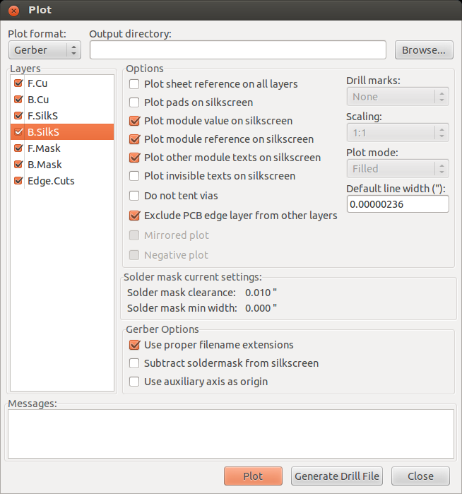
To generate the gerber and drill files for production, click on the Plot toolbar button in PCBNEW. It is located in the top toolbar and looks like a printer with a “P” overlaid. This brings up the plot dialog box. (Click to enlarge image.)

gerbers_01_plot

Here, ensure that the “Plot format” is “Gerber”. Leave the “Output directory” field blank, and it will default to saving the files into the project directory. Make sure you check all the layers you want to send to production. If you didn’t use back-side silkscreen, or don’t want to use any back-side silkscreen (some places charge extra for that), you can un-check the B.SilkS layer. The other checkmark boxes are the defaults, but ensure that “Exclude PCB edge layer from other layers” and “Use proper filename extensions” are checked. Press “Plot” to generate the files, one per layer. You will see output in the “Messages:” box at the bottom. When that is finished, click “Generate Drill File” to bring up the next dialog box. (Click to enlarge image.)

gerbers_02_drill

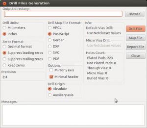
Again, leave the “Output directory” text field empty. The settings here are very important, especially the Drill Units (Inches), Zeros Format (Suppress leading zeros), and Options (Minimal header). You absolutely must check “Minimal header” and un-check “Mirror Y-Axis”. Since we aren’t making a drill map, the “Drill Map File Format” option doesn’t matter. Click the “Drill File” button to generate the drill file. Then press “Close” and “Close”.

Now you can zip up the generated gerber/drill files and send them off for fabrication. At Wayne and Layne, we really like the prototype PCB fabrication services from OSH Park. They describe themselves as

This is a community printed circuit board (PCB) order. We take designs from lots of people, put them all together on a panel and then order the panel from a fab. Since we’re all splitting the panel setup cost, this lets us make circuit boards inexpensively.

This service grew out of the DorkbotPDX PCB Order run by @laen and now comprises of a two-layer panel every other day, a four-layer panel every three weeks and a periodic two-layer medium run service for people needing more than 150 square inches of board.

They have very inexpensive rates, decent production time, and very high-quality output. Plus, the gold and purple boards just look very nice! Here are the details about pricing and design rules (minimum clearance and trace width, minimum hole size, etc).


Other tutorials in this series:


  • Newsletter

    Sign up for the PlanetArduino Newsletter, which delivers the most popular articles via e-mail to your inbox every week. Just fill in the information below and submit.

  • Like Us on Facebook