Posts | Comments

Planet Arduino

Archive for the ‘digital’ Category

Jul
02

Tutorial – Arduino and the TI ADS1110 16-bit ADC

ADC, ads1110, analogue, arduino, converter, digital, i2c, instruments, texas, TI, tronixstuff, tutorial Comments Off on Tutorial – Arduino and the TI ADS1110 16-bit ADC 

Learn how to use the TI ADS1110 16-bit ADC with Arduino in chapter fifty-three of my Arduino Tutorials. The first chapter is here, the complete series is detailed here.

Updated 02/07/2013

Introduction

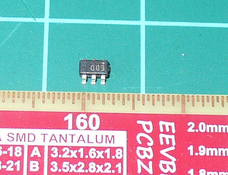
Moving on from the last chapter where we explained an 8-bit ADC, in this instalment we have the Texas Instruments ADS1110 – an incredibly tiny but useful 16-bit analogue-to-digital converter IC.  It can operate between 2.7 and 5.5 V so it’s also fine for Arduino Due and other lower-voltage development boards. This is a quick guide to get you going with the ADS1110 ready for further applications. Before continuing any further, please download the data sheet (pdf) as it will be useful and referred to during this tutorial. The ADS1110 gives you the option of a more accurate ADC than offered by the Arduino’s 10-bit ADCs – and it’s relatively easy to use. The only block for some is the package type – it’s only available in SOT23-6:
So unless you’re making a customised PCB, some sort of breakout will be required. One useful example is the Schmartboard we reviewed earlier:

ads1110schmartboard

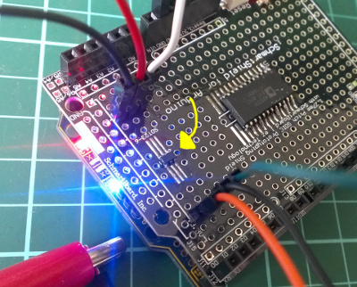
The ADS1110 uses the I2C bus for communication, so if this is new to you – please review the I2C tutorials before continuing. And as there’s only six pins you can’t set the bus address – instead, you can select from six variants of the ADS1110 – each with their own address (see page two of the data sheet). As you can see the in the photo above, ours is marked “EDO” which matches to the bus address 1001000 or 0x48h. And with the example circuits we’ve used 10kΩ pull-up resistors on the I2C bus. You can use the ADS1110 as either a single-ended or differential ADC –  But first we need to examine the configuration register which is used to control various attributes, and the data register.

Configuration register

Turn to page eleven of the data sheet. The configuration register is one byte in size, and as the ADS1110 resets on a power-cycle – you need to reset the register if your needs are different to the defaults. The data sheet spells it out quite neatly… bits 0 and 1 determine the gain setting for the PGA (programmable gain amplifier). If you’re just measuring voltages or experimenting, leave these as zero for a gain of 1V/V. Next, the data rate for the ADS1110 is controlled with bits 2 and 3. If you have continuous sampling turned on, this determines the number of samples per second taken by the ADC.

After some experimenting with an Arduino Uno we found the values returned from the ADC were a bit off when using the fastest rate, so leave it as 15 SPS unless required otherwise. Bit 4 sets either continuous sampling (0) or one-off sampling (1). Ignore bits 5 and 6, however they’re always set as 0. Finally bit 7 – if you’re in one-off sampling mode, setting it to 1 requests a sample – and reading it will tell you if the returned data is new (0) or old (1). You can check that the value measured is a new value – if the first bit of the configuration byte that comes after the data is 0, it’s new. If it returns 1 the ADC conversion hasn’t finished.

Data register

As the ADS1110 is a 16-bit ADC, it returns the data over two bytes – and then follows with the value of the configuration register. So if you request three bytes the whole lot comes back. The data is in “two’s complement” form, which is a method of using signed numbers with binary. Converting those two bytes is done by some simple maths. When sampling at 15 SPS, the value returned by the ADS1110 (not the voltage)  falls between -32768 and 32767. The higher byte of the value is multiplied by 256, then added to the lower byte – which is then multiplied by 2.048 and finally divided by 32767. Don’t panic, as we do this in the example sketch below.

Single-ended ADC mode

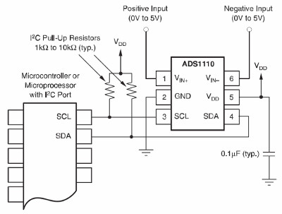
In this mode you can read a voltage that falls between zero and 2.048 V (which also happens to be the inbuilt reference voltage for the ADS1110). The example circuit is simple (from the data sheet):
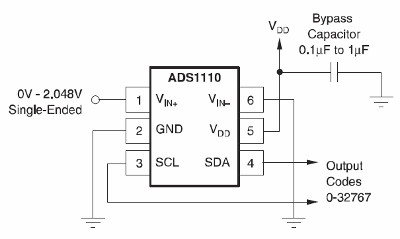
singledemoDon’t forget the 10kΩ pull-up resistors on the I2C bus. The following sketch uses the ADS1110 in the default mode, and simply returns the voltage measured (download):

// Example 53.1 - ADS1110 single-sided voltmeter (0~2.048VDC)
#include "Wire.h"
#define ads1110 0x48
float voltage, data; 
byte highbyte, lowbyte, configRegister;
void setup() 
{ 
 Serial.begin(9600); 
 Wire.begin(); 
}
void loop() 
{ 
 Wire.requestFrom(ads1110, 3); 
 while(Wire.available()) // ensure all the data comes in 
 { 
 highbyte = Wire.read(); // high byte * B11111111
 lowbyte = Wire.read(); // low byte
 configRegister = Wire.read(); 
 } 

 data = highbyte * 256; 
 data = data + lowbyte;
 Serial.print("Data >> "); 
 Serial.println(data, DEC); 
 Serial.print("Voltage >> "); 
 voltage = data * 2.048 ;
 voltage = voltage / 32767.0; 
 Serial.print(voltage, DEC); 
 Serial.println(" V"); 
 delay(1000);
}

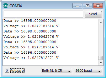
Once uploaded, connect the signal to measure and open the serial monitor – you’ll be presented with something similar to:

singledemosm

If you need to alter the gain of the internal programmable gain amplifier of the ADC – you’ll need to write a new byte into the configuration register using:

 Wire.beginTransmission(ads1110);
 Wire.write(configuration byte); 
 Wire.endTransmission();

before requesting the ADC data. This would be 0x8D, 0x8E or 0x8F for gain values of 2, 4 and 8 respectively – and use 0x8C to reset the ADS1110 back to default.

Differential ADC mode

In this mode you can read the difference between two voltages that each fall between zero and 5 V. The example circuit is simple (from the data sheet):

diffcircuit

We must note here (and in the data sheet) that the ADS1110 can’t accept negative voltages on either of the inputs. You can use the previous sketch for the same results – and the resulting voltage will be the value of Vin- subtracted from Vin+. For example, if you had 2 V on Vin+ and 1 V on Vin- the resulting voltage would be 1 V (with the gain set to 1).

Conclusion

Once again I hope you found this of interest, and possibly useful. And if you enjoy my tutorials, or want to introduce someone else to the interesting world of Arduino – check out my new book “Arduino Workshop” from No Starch Press.

In the meanwhile have fun and keep checking into tronixstuff.com. Why not follow things on twitterGoogle+, subscribe  for email updates or RSS using the links on the right-hand column? And join our friendly Google Group – dedicated to the projects and related items on this website. Sign up – it’s free, helpful to each other –  and we can all learn something.


Jul
02

Tutorial – Arduino and the TI ADS1110 16-bit ADC

ADC, ads1110, analogue, arduino, converter, digital, i2c, instruments, lesson, texas, TI, tronixstuff, tutorial Comments Off on Tutorial – Arduino and the TI ADS1110 16-bit ADC 

Learn how to use the TI ADS1110 16-bit ADC with Arduino in chapter fifty-three of my Arduino Tutorials. The first chapter is here, the complete series is detailed here.

Updated 02/07/2013

Introduction

Moving on from the last chapter where we explained an 8-bit ADC, in this instalment we have the Texas Instruments ADS1110 – an incredibly tiny but useful 16-bit analogue-to-digital converter IC.  It can operate between 2.7 and 5.5 V so it’s also fine for Arduino Due and other lower-voltage development boards. This is a quick guide to get you going with the ADS1110 ready for further applications. Before continuing any further, please download the data sheet (pdf) as it will be useful and referred to during this tutorial. The ADS1110 gives you the option of a more accurate ADC than offered by the Arduino’s 10-bit ADCs – and it’s relatively easy to use. The only block for some is the package type – it’s only available in SOT23-6:

So unless you’re making a customised PCB, some sort of breakout will be required. One useful example is the Schmartboard we reviewed earlier:

ads1110schmartboard

The ADS1110 uses the I2C bus for communication, so if this is new to you – please review the I2C tutorials before continuing. And as there’s only six pins you can’t set the bus address – instead, you can select from six variants of the ADS1110 – each with their own address (see page two of the data sheet). As you can see the in the photo above, ours is marked “EDO” which matches to the bus address 1001000 or 0x48h. And with the example circuits we’ve used 10kΩ pull-up resistors on the I2C bus. You can use the ADS1110 as either a single-ended or differential ADC –  But first we need to examine the configuration register which is used to control various attributes, and the data register.

Configuration register

Turn to page eleven of the data sheet. The configuration register is one byte in size, and as the ADS1110 resets on a power-cycle – you need to reset the register if your needs are different to the defaults. The data sheet spells it out quite neatly… bits 0 and 1 determine the gain setting for the PGA (programmable gain amplifier). If you’re just measuring voltages or experimenting, leave these as zero for a gain of 1V/V. Next, the data rate for the ADS1110 is controlled with bits 2 and 3. If you have continuous sampling turned on, this determines the number of samples per second taken by the ADC.

After some experimenting with an Arduino Uno we found the values returned from the ADC were a bit off when using the fastest rate, so leave it as 15 SPS unless required otherwise. Bit 4 sets either continuous sampling (0) or one-off sampling (1). Ignore bits 5 and 6, however they’re always set as 0. Finally bit 7 – if you’re in one-off sampling mode, setting it to 1 requests a sample – and reading it will tell you if the returned data is new (0) or old (1). You can check that the value measured is a new value – if the first bit of the configuration byte that comes after the data is 0, it’s new. If it returns 1 the ADC conversion hasn’t finished.

Data register

As the ADS1110 is a 16-bit ADC, it returns the data over two bytes – and then follows with the value of the configuration register. So if you request three bytes the whole lot comes back. The data is in “two’s complement” form, which is a method of using signed numbers with binary. Converting those two bytes is done by some simple maths. When sampling at 15 SPS, the value returned by the ADS1110 (not the voltage)  falls between -32768 and 32767. The higher byte of the value is multiplied by 256, then added to the lower byte – which is then multiplied by 2.048 and finally divided by 32768. Don’t panic, as we do this in the example sketch below.

Single-ended ADC mode

In this mode you can read a voltage that falls between zero and 2.048 V (which also happens to be the inbuilt reference voltage for the ADS1110). The example circuit is simple (from the data sheet):

singledemoDon’t forget the 10kΩ pull-up resistors on the I2C bus. The following sketch uses the ADS1110 in the default mode, and simply returns the voltage measured:

// Example 53.1 - ADS1110 single-sided voltmeter (0~2.048VDC)

#include "Wire.h"
#define ads1110 0x48
float voltage, data;
byte highbyte, lowbyte, configRegister;
void setup()
{
 Serial.begin(9600);
 Wire.begin();
}
void loop()
{
 Wire.requestFrom(ads1110, 3);
 while(Wire.available()) // ensure all the data comes in
 {
 highbyte = Wire.read(); // high byte * B11111111
 lowbyte = Wire.read(); // low byte
 configRegister = Wire.read();
 }

 data = highbyte * 256;
 data = data + lowbyte;
 Serial.print("Data >> ");
 Serial.println(data, DEC);
 Serial.print("Voltage >> ");
 voltage = data * 2.048 ;
 voltage = voltage / 32768.0;
 Serial.print(voltage, DEC);
 Serial.println(" V");
 delay(1000);
}

Once uploaded, connect the signal to measure and open the serial monitor – you’ll be presented with something similar to:

singledemosm

If you need to alter the gain of the internal programmable gain amplifier of the ADC – you’ll need to write a new byte into the configuration register using:

Wire.beginTransmission(ads1110);
Wire.write(configuration byte); 
Wire.endTransmission();

before requesting the ADC data. This would be 0x8D, 0x8E or 0x8F for gain values of 2, 4 and 8 respectively – and use 0x8C to reset the ADS1110 back to default.

Differential ADC mode

In this mode you can read the difference between two voltages that each fall between zero and 5 V. The example circuit is simple (from the data sheet):

diffcircuit

We must note here (and in the data sheet) that the ADS1110 can’t accept negative voltages on either of the inputs. You can use the previous sketch for the same results – and the resulting voltage will be the value of Vin- subtracted from Vin+. For example, if you had 2 V on Vin+ and 1 V on Vin- the resulting voltage would be 1 V (with the gain set to 1).

Conclusion

Once again I hope you found this of interest, and possibly useful. And if you enjoy my tutorials, or want to introduce someone else to the interesting world of Arduino – check out my new book “Arduino Workshop” from No Starch Press.

LEDborder

In the meanwhile have fun and keep checking into tronixstuff.com. Why not follow things on twitterGoogle+, subscribe  for email updates or RSS using the links on the right-hand column? And join our friendly Google Group – dedicated to the projects and related items on this website. Sign up – it’s free, helpful to each other –  and we can all learn something.
The post Tutorial – Arduino and the TI ADS1110 16-bit ADC appeared first on tronixstuff.

Learn how to use the NXP PCF 8591 8-bit A/D and D/A IC with Arduino in chapter fifty-two of my Arduino Tutorials. The first chapter is here, the complete series is detailed here.

Updated 17/06/2013

Introduction

Have you ever wanted more analogue input pins on your Arduino project, but not wanted to fork out for a Mega? Or would you like to generate analogue signals? Then check out the subject of our tutorial – the NXP PCF8591 IC. It solves both these problems as it has a single DAC (digital to analogue) converter as well as four ADCs (analogue to digital converters) – all accessible via the I2C bus. If the I2C bus is new to you, please familiarise yourself with the readings here before moving forward.

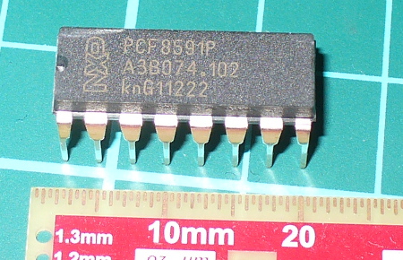
The PCF8591 is available in DIP form, which makes it easy to experiment with:

pcf8591

You can get them from the usual retailers. Before moving on, download the data sheet. The PCF8591 can operate on both 5V and 3.3V so if you’re using an Arduino Due, Raspberry Pi or other 3.3 V development board you’re fine. Now we’ll first explain the DAC, then the ADCs.

Using the DAC (digital-to-analogue converter)

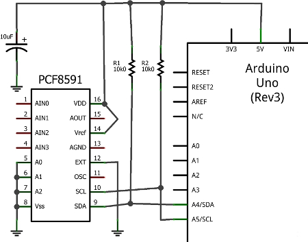
The DAC on the PCF8591 has a resolution of 8-bits – so it can generate a theoretical signal of between zero volts and the reference voltage (Vref) in 255 steps. For demonstration purposes we’ll use a Vref of 5V, and you can use a lower Vref such as 3.3V or whatever you wish the maximum value to be … however it must be less than the supply voltage. Note that when there is a load on the analogue output (a real-world situation), the maximum output voltage will drop – the data sheet (which you downloaded) shows a 10% drop for a 10kΩ load. Now for our demonstration circuit:

pcf8591basic_schem

Note the use of 10kΩ pull-up resistors on the I2C bus, and the 10μF capacitor between 5V and GND. The I2C bus address is set by a combination of pins A0~A2, and with them all to GND the address is 0×90. The analogue output can be taken from pin 15 (and there’s a seperate analogue GND on pin 13. Also, connect pin 13 to GND, and circuit GND to Arduino GND.

To control the DAC we need to send two bytes of data. The first is the control byte, which simply activates the DAC and is 1000000 (or 0×40) and the next byte is the value between 0 and 255 (the output level). This is demonstrated in the following sketch (download):

// Example 52.1 PCF8591 DAC demo
// http://tronixstuff.com/tutorials Chapter 52
// John Boxall June 2013
#include "Wire.h"
#define PCF8591 (0x90 >> 1) // I2C bus address
void setup()
{
 Wire.begin();
}
void loop()
{ 
 for (int i=0; i<256; i++)
 {
 Wire.beginTransmission(PCF8591); // wake up PCF8591
 Wire.write(0x40); // control byte - turn on DAC (binary 1000000)
 Wire.write(i); // value to send to DAC
 Wire.endTransmission(); // end tranmission
 }

 for (int i=255; i>=0; --i)
 {
 Wire.beginTransmission(PCF8591); // wake up PCF8591
 Wire.write(0x40); // control byte - turn on DAC (binary 1000000)
 Wire.write(i); // value to send to DAC
 Wire.endTransmission(); // end tranmission
 }
}

Did you notice the bit shift of the bus address in the #define statement? Arduino sends 7-bit addresses but the PCF8591 wants an 8-bit, so we shift the byte over by one bit. 

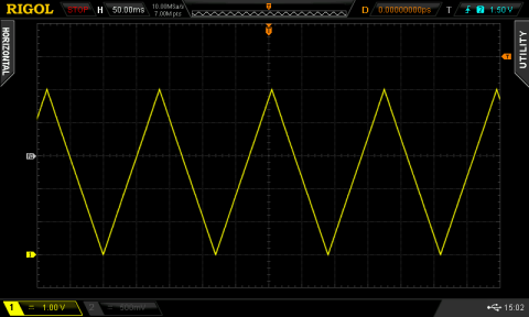
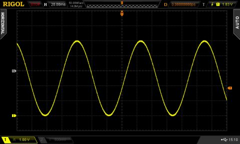
The results of the sketch are shown below, we’ve connected the Vref to 5V and the oscilloscope probe and GND to the analogue output and GND respectively (click image to enlarge):

triangle

If you like curves you can generate sine waves with the sketch below. It uses a lookup table in an array which contains the necessary pre-calculated data points (download):

// Example 52.2 PCF8591 DAC demo - sine wave
// http://tronixstuff.com/tutorials Chapter 52
// John Boxall June 2013
#include "Wire.h"
#define PCF8591 (0x90 >> 1) // I2C bus address
uint8_t sine_wave[256] = {
 0x80, 0x83, 0x86, 0x89, 0x8C, 0x90, 0x93, 0x96,
 0x99, 0x9C, 0x9F, 0xA2, 0xA5, 0xA8, 0xAB, 0xAE,
 0xB1, 0xB3, 0xB6, 0xB9, 0xBC, 0xBF, 0xC1, 0xC4,
 0xC7, 0xC9, 0xCC, 0xCE, 0xD1, 0xD3, 0xD5, 0xD8,
 0xDA, 0xDC, 0xDE, 0xE0, 0xE2, 0xE4, 0xE6, 0xE8,
 0xEA, 0xEB, 0xED, 0xEF, 0xF0, 0xF1, 0xF3, 0xF4,
 0xF5, 0xF6, 0xF8, 0xF9, 0xFA, 0xFA, 0xFB, 0xFC,
 0xFD, 0xFD, 0xFE, 0xFE, 0xFE, 0xFF, 0xFF, 0xFF,
 0xFF, 0xFF, 0xFF, 0xFF, 0xFE, 0xFE, 0xFE, 0xFD,
 0xFD, 0xFC, 0xFB, 0xFA, 0xFA, 0xF9, 0xF8, 0xF6,
 0xF5, 0xF4, 0xF3, 0xF1, 0xF0, 0xEF, 0xED, 0xEB,
 0xEA, 0xE8, 0xE6, 0xE4, 0xE2, 0xE0, 0xDE, 0xDC,
 0xDA, 0xD8, 0xD5, 0xD3, 0xD1, 0xCE, 0xCC, 0xC9,
 0xC7, 0xC4, 0xC1, 0xBF, 0xBC, 0xB9, 0xB6, 0xB3,
 0xB1, 0xAE, 0xAB, 0xA8, 0xA5, 0xA2, 0x9F, 0x9C,
 0x99, 0x96, 0x93, 0x90, 0x8C, 0x89, 0x86, 0x83,
 0x80, 0x7D, 0x7A, 0x77, 0x74, 0x70, 0x6D, 0x6A,
 0x67, 0x64, 0x61, 0x5E, 0x5B, 0x58, 0x55, 0x52,
 0x4F, 0x4D, 0x4A, 0x47, 0x44, 0x41, 0x3F, 0x3C,
 0x39, 0x37, 0x34, 0x32, 0x2F, 0x2D, 0x2B, 0x28,
 0x26, 0x24, 0x22, 0x20, 0x1E, 0x1C, 0x1A, 0x18,
 0x16, 0x15, 0x13, 0x11, 0x10, 0x0F, 0x0D, 0x0C,
 0x0B, 0x0A, 0x08, 0x07, 0x06, 0x06, 0x05, 0x04,
 0x03, 0x03, 0x02, 0x02, 0x02, 0x01, 0x01, 0x01,
 0x01, 0x01, 0x01, 0x01, 0x02, 0x02, 0x02, 0x03,
 0x03, 0x04, 0x05, 0x06, 0x06, 0x07, 0x08, 0x0A,
 0x0B, 0x0C, 0x0D, 0x0F, 0x10, 0x11, 0x13, 0x15,
 0x16, 0x18, 0x1A, 0x1C, 0x1E, 0x20, 0x22, 0x24,
 0x26, 0x28, 0x2B, 0x2D, 0x2F, 0x32, 0x34, 0x37,
 0x39, 0x3C, 0x3F, 0x41, 0x44, 0x47, 0x4A, 0x4D,
 0x4F, 0x52, 0x55, 0x58, 0x5B, 0x5E, 0x61, 0x64,
 0x67, 0x6A, 0x6D, 0x70, 0x74, 0x77, 0x7A, 0x7D
};
void setup()
{
 Wire.begin();
}
void loop()
{ 
 for (int i=0; i<256; i++)
 {
 Wire.beginTransmission(PCF8591); // wake up PCF8591
 Wire.write(0x40); // control byte - turn on DAC (binary 1000000)
 Wire.write(sine_wave[i]); // value to send to DAC
 Wire.endTransmission(); // end tranmission
 }
}

And the results (click image to enlarge):

sine

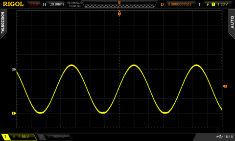
For the following DSO image dump, we changed the Vref to 3.3V – note the change in the maxima on the sine wave:

sine3v3

Now you can experiment with the DAC to make sound effects, signals or control other analogue circuits.

Using the ADCs (analogue-to-digital converters)

If you’ve used the analogRead() function on your Arduino (way back in Chapter One) then you’re already familiar with an ADC. With out PCF8591 we can read a voltage between zero and the Vref and it will return a value of between zero and 255 which is directly proportional to zero and the Vref. For example, measuring 3.3V should return 168. The resolution (8-bit) of the ADC is lower than the onboard Arduino (10-bit) however the PCF8591 can do something the Arduino’s ADC cannot. But we’ll get to that in a moment.

First, to simply read the values of each ADC pin we send a control byte to tell the PCF8591 which ADC we want to read. For ADCs zero to three the control byte is 0×00, 0×01, ox02 and 0×03 respectively. Then we ask for two bytes of data back from the ADC, and store the second byte for use. Why two bytes? The PCF8591 returns the previously measured value first – then the current byte. (See Figure 8 in the data sheet). Finally, if you’re not using all the ADC pins, connect the unused ones to GND.

The following example sketch simply retrieves values from each ADC pin one at a time, then displays them in the serial monitor (download):

// Example 52.3 PCF8591 ADC demo 
// http://tronixstuff.com/tutorials Chapter 52
// John Boxall June 2013
#include "Wire.h"
#define PCF8591 (0x90 >> 1) // I2C bus address
#define ADC0 0x00 // control bytes for reading individual ADCs
#define ADC1 0x01
#define ADC2 0x02
#define ADC3 0x03
byte value0, value1, value2, value3;
void setup()
{
 Wire.begin();
 Serial.begin(9600);
}
void loop()
{ 
 Wire.beginTransmission(PCF8591); // wake up PCF8591
 Wire.write(ADC0); // control byte - read ADC0
 Wire.endTransmission(); // end tranmission
 Wire.requestFrom(PCF8591, 2);
 value0=Wire.read();
 value0=Wire.read();
 Wire.beginTransmission(PCF8591); // wake up PCF8591
 Wire.write(ADC1); // control byte - read ADC1
 Wire.endTransmission(); // end tranmission
 Wire.requestFrom(PCF8591, 2);
 value1=Wire.read();
 value1=Wire.read();
 Wire.beginTransmission(PCF8591); // wake up PCF8591
 Wire.write(ADC2); // control byte - read ADC2
 Wire.endTransmission(); // end tranmission
 Wire.requestFrom(PCF8591, 2);
 value2=Wire.read();
 value2=Wire.read();
 Wire.beginTransmission(PCF8591); // wake up PCF8591
 Wire.write(ADC3); // control byte - read ADC3
 Wire.endTransmission(); // end tranmission
 Wire.requestFrom(PCF8591, 2);
 value3=Wire.read();
 value3=Wire.read();
 Serial.print(value0); Serial.print(" ");
 Serial.print(value1); Serial.print(" ");
 Serial.print(value2); Serial.print(" ");
 Serial.print(value3); Serial.print(" "); 
 Serial.println();
}

Upon running the sketch you’ll be presented with the values of each ADC in the serial monitor. Although it was a simple demonstration to show you how to individually read each ADC, it is a cumbersome method of getting more than one byte at a time from a particular ADC.

To do this, change the control byte to request auto-increment, which is done by setting bit 2 of the control byte to 1. So to start from ADC0 we use a new control byte of binary 00000100 or hexadecimal 0×04. Then request five bytes of data (once again we ignore the first byte) which will cause the PCF8591 to return all values in one chain of bytes. This process is demonstrated in the following sketch (download):

// Example 52.4 PCF8591 ADC demo 
// http://tronixstuff.com/tutorials Chapter 52
// John Boxall June 2013
#include "Wire.h"
#define PCF8591 (0x90 >> 1) // I2C bus address
byte value0, value1, value2, value3;
void setup()
{
 Wire.begin();
 Serial.begin(9600);
}
void loop()
{ 
 Wire.beginTransmission(PCF8591); // wake up PCF8591
 Wire.write(0x04); // control byte - read ADC0 then auto-increment
 Wire.endTransmission(); // end tranmission
 Wire.requestFrom(PCF8591, 5); 
 value0=Wire.read();
 value0=Wire.read(); 
 value1=Wire.read(); 
 value2=Wire.read(); 
 value3=Wire.read();
 Serial.print(value0); Serial.print(" ");
 Serial.print(value1); Serial.print(" ");
 Serial.print(value2); Serial.print(" ");
 Serial.print(value3); Serial.print(" "); 
 Serial.println();
}

Previously we mentioned that the PCF8591 can do something that the Arduino’s ADC cannot, and this is offer a differential ADC. As opposed to the Arduino’s single-ended (i.e. it returns the difference between the positive signal voltage and GND, the differential ADC accepts two signals (that don’t necessarily have to be referenced to ground), and returns the difference between the two signals. This can be convenient for measuring small changes in voltages for load cells and so on.

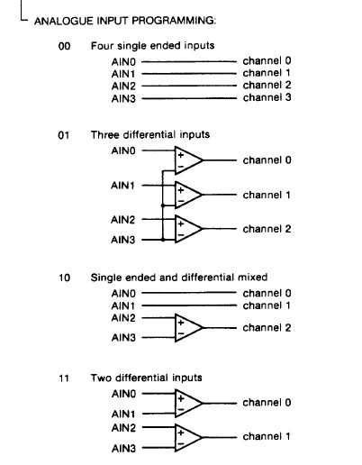
Setting up the PCF8591 for differential ADC is a simple matter of changing the control byte. If you turn to page seven of the data sheet, then consider the different types of analogue input programming. Previously we used mode ’00′ for four inputs, however you can select the others which are clearly illustrated, for example:

adcmodes

So to set the control byte for two differential inputs, use binary 00110000 or 0×30. Then it’s a simple matter of requesting the bytes of data and working with them. As you can see there’s also combination single/differential and a complex three-differential input. However we’ll leave them for the time being.

Conclusion

Hopefully you found this of interest, whether adding a DAC to your experiments or learning a bit more about ADCs. We’ll have some more analogue to digital articles coming up soon, so stay tuned. And if you enjoy my tutorials, or want to introduce someone else to the interesting world of Arduino – check out my new book “Arduino Workshop” from No Starch Press.

In the meanwhile have fun and keep checking into tronixstuff.com. Why not follow things on twitterGoogle+, subscribe  for email updates or RSS using the links on the right-hand column? And join our friendly Google Group – dedicated to the projects and related items on this website. Sign up – it’s free, helpful to each other –  and we can all learn something.

Learn how to use the NXP PCF 8591 8-bit A/D and D/A IC with Arduino in chapter fifty-two of my Arduino Tutorials. The first chapter is here, the complete series is detailed here.

Updated 17/06/2013

Introduction

Have you ever wanted more analogue input pins on your Arduino project, but not wanted to fork out for a Mega? Or would you like to generate analogue signals? Then check out the subject of our tutorial – the NXP PCF8591 IC. It solves both these problems as it has a single DAC (digital to analogue) converter as well as four ADCs (analogue to digital converters) – all accessible via the I2C bus. If the I2C bus is new to you, please familiarise yourself with the readings here before moving forward.

The PCF8591 is available in DIP form, which makes it easy to experiment with:

pcf8591

You can get them from the usual retailers. Before moving on, download the data sheet. The PCF8591 can operate on both 5V and 3.3V so if you’re using an Arduino Due, Raspberry Pi or other 3.3 V development board you’re fine. Now we’ll first explain the DAC, then the ADCs.

Using the DAC (digital-to-analogue converter)

The DAC on the PCF8591 has a resolution of 8-bits – so it can generate a theoretical signal of between zero volts and the reference voltage (Vref) in 255 steps. For demonstration purposes we’ll use a Vref of 5V, and you can use a lower Vref such as 3.3V or whatever you wish the maximum value to be … however it must be less than the supply voltage. Note that when there is a load on the analogue output (a real-world situation), the maximum output voltage will drop – the data sheet (which you downloaded) shows a 10% drop for a 10kΩ load. Now for our demonstration circuit:

pcf8591basic_schem

Note the use of 10kΩ pull-up resistors on the I2C bus, and the 10μF capacitor between 5V and GND. The I2C bus address is set by a combination of pins A0~A2, and with them all to GND the address is 0×90. The analogue output can be taken from pin 15 (and there’s a seperate analogue GND on pin 13. Also, connect pin 13 to GND, and circuit GND to Arduino GND.

To control the DAC we need to send two bytes of data. The first is the control byte, which simply activates the DAC and is 1000000 (or 0×40) and the next byte is the value between 0 and 255 (the output level). This is demonstrated in the following sketch:

// Example 52.1 PCF8591 DAC demo
// http://tronixstuff.com/tutorials Chapter 52
// John Boxall June 2013
#include "Wire.h"
#define PCF8591 (0x90 >> 1) // I2C bus address
void setup()
{
 Wire.begin();
}
void loop()
{
 for (int i=0; i<256; i++)
 {
 Wire.beginTransmission(PCF8591); // wake up PCF8591
 Wire.write(0x40); // control byte - turn on DAC (binary 1000000)
 Wire.write(i); // value to send to DAC
 Wire.endTransmission(); // end tranmission
 }

 for (int i=255; i>=0; --i)
 {
 Wire.beginTransmission(PCF8591); // wake up PCF8591
 Wire.write(0x40); // control byte - turn on DAC (binary 1000000)
 Wire.write(i); // value to send to DAC
 Wire.endTransmission(); // end tranmission
 }
}

Did you notice the bit shift of the bus address in the #define statement? Arduino sends 7-bit addresses but the PCF8591 wants an 8-bit, so we shift the byte over by one bit. 

The results of the sketch are shown below, we’ve connected the Vref to 5V and the oscilloscope probe and GND to the analogue output and GND respectively:

triangle

If you like curves you can generate sine waves with the sketch below. It uses a lookup table in an array which contains the necessary pre-calculated data points:

// Example 52.2 PCF8591 DAC demo - sine wave
// http://tronixstuff.com/tutorials Chapter 52
// John Boxall June 2013

#include "Wire.h"
#define PCF8591 (0x90 >> 1) // I2C bus address

uint8_t sine_wave[256] = {
 0x80, 0x83, 0x86, 0x89, 0x8C, 0x90, 0x93, 0x96,
 0x99, 0x9C, 0x9F, 0xA2, 0xA5, 0xA8, 0xAB, 0xAE,
 0xB1, 0xB3, 0xB6, 0xB9, 0xBC, 0xBF, 0xC1, 0xC4,
 0xC7, 0xC9, 0xCC, 0xCE, 0xD1, 0xD3, 0xD5, 0xD8,
 0xDA, 0xDC, 0xDE, 0xE0, 0xE2, 0xE4, 0xE6, 0xE8,
 0xEA, 0xEB, 0xED, 0xEF, 0xF0, 0xF1, 0xF3, 0xF4,
 0xF5, 0xF6, 0xF8, 0xF9, 0xFA, 0xFA, 0xFB, 0xFC,
 0xFD, 0xFD, 0xFE, 0xFE, 0xFE, 0xFF, 0xFF, 0xFF,
 0xFF, 0xFF, 0xFF, 0xFF, 0xFE, 0xFE, 0xFE, 0xFD,
 0xFD, 0xFC, 0xFB, 0xFA, 0xFA, 0xF9, 0xF8, 0xF6,
 0xF5, 0xF4, 0xF3, 0xF1, 0xF0, 0xEF, 0xED, 0xEB,
 0xEA, 0xE8, 0xE6, 0xE4, 0xE2, 0xE0, 0xDE, 0xDC,
 0xDA, 0xD8, 0xD5, 0xD3, 0xD1, 0xCE, 0xCC, 0xC9,
 0xC7, 0xC4, 0xC1, 0xBF, 0xBC, 0xB9, 0xB6, 0xB3,
 0xB1, 0xAE, 0xAB, 0xA8, 0xA5, 0xA2, 0x9F, 0x9C,
 0x99, 0x96, 0x93, 0x90, 0x8C, 0x89, 0x86, 0x83,
 0x80, 0x7D, 0x7A, 0x77, 0x74, 0x70, 0x6D, 0x6A,
 0x67, 0x64, 0x61, 0x5E, 0x5B, 0x58, 0x55, 0x52,
 0x4F, 0x4D, 0x4A, 0x47, 0x44, 0x41, 0x3F, 0x3C,
 0x39, 0x37, 0x34, 0x32, 0x2F, 0x2D, 0x2B, 0x28,
 0x26, 0x24, 0x22, 0x20, 0x1E, 0x1C, 0x1A, 0x18,
 0x16, 0x15, 0x13, 0x11, 0x10, 0x0F, 0x0D, 0x0C,
 0x0B, 0x0A, 0x08, 0x07, 0x06, 0x06, 0x05, 0x04,
 0x03, 0x03, 0x02, 0x02, 0x02, 0x01, 0x01, 0x01,
 0x01, 0x01, 0x01, 0x01, 0x02, 0x02, 0x02, 0x03,
 0x03, 0x04, 0x05, 0x06, 0x06, 0x07, 0x08, 0x0A,
 0x0B, 0x0C, 0x0D, 0x0F, 0x10, 0x11, 0x13, 0x15,
 0x16, 0x18, 0x1A, 0x1C, 0x1E, 0x20, 0x22, 0x24,
 0x26, 0x28, 0x2B, 0x2D, 0x2F, 0x32, 0x34, 0x37,
 0x39, 0x3C, 0x3F, 0x41, 0x44, 0x47, 0x4A, 0x4D,
 0x4F, 0x52, 0x55, 0x58, 0x5B, 0x5E, 0x61, 0x64,
 0x67, 0x6A, 0x6D, 0x70, 0x74, 0x77, 0x7A, 0x7D
};
void setup()
{
 Wire.begin();
}
void loop()
{
 for (int i=0; i<256; i++)
 {
 Wire.beginTransmission(PCF8591); // wake up PCF8591
 Wire.write(0x40); // control byte - turn on DAC (binary 1000000)
 Wire.write(sine_wave[i]); // value to send to DAC
 Wire.endTransmission(); // end tranmission
 }
}

And the results:

sine

For the following DSO image dump, we changed the Vref to 3.3V – note the change in the maxima on the sine wave:

sine3v3

Now you can experiment with the DAC to make sound effects, signals or control other analogue circuits.

Using the ADCs (analogue-to-digital converters)

If you’ve used the analogRead() function on your Arduino (way back in Chapter One) then you’re already familiar with an ADC. With out PCF8591 we can read a voltage between zero and the Vref and it will return a value of between zero and 255 which is directly proportional to zero and the Vref. For example, measuring 3.3V should return 168. The resolution (8-bit) of the ADC is lower than the onboard Arduino (10-bit) however the PCF8591 can do something the Arduino’s ADC cannot. But we’ll get to that in a moment.

First, to simply read the values of each ADC pin we send a control byte to tell the PCF8591 which ADC we want to read. For ADCs zero to three the control byte is 0×00, 0×01, ox02 and 0×03 respectively. Then we ask for two bytes of data back from the ADC, and store the second byte for use. Why two bytes? The PCF8591 returns the previously measured value first – then the current byte. (See Figure 8 in the data sheet). Finally, if you’re not using all the ADC pins, connect the unused ones to GND.

The following example sketch simply retrieves values from each ADC pin one at a time, then displays them in the serial monitor:

// Example 52.3 PCF8591 ADC demo
// http://tronixstuff.com/tutorials Chapter 52
// John Boxall June 2013
#include "Wire.h"
#define PCF8591 (0x90 >> 1) // I2C bus address
#define ADC0 0x00 // control bytes for reading individual ADCs
#define ADC1 0x01
#define ADC2 0x02
#define ADC3 0x03
byte value0, value1, value2, value3;
void setup()
{
 Wire.begin();
 Serial.begin(9600);
}
void loop()
{
 Wire.beginTransmission(PCF8591); // wake up PCF8591
 Wire.write(ADC0); // control byte - read ADC0
 Wire.endTransmission(); // end tranmission
 Wire.requestFrom(PCF8591, 2);
 value0=Wire.read();
 value0=Wire.read();
 Wire.beginTransmission(PCF8591); // wake up PCF8591
 Wire.write(ADC1); // control byte - read ADC1
 Wire.endTransmission(); // end tranmission
 Wire.requestFrom(PCF8591, 2);
 value1=Wire.read();
 value1=Wire.read();
 Wire.beginTransmission(PCF8591); // wake up PCF8591
 Wire.write(ADC2); // control byte - read ADC2
 Wire.endTransmission(); // end tranmission
 Wire.requestFrom(PCF8591, 2);
 value2=Wire.read();
 value2=Wire.read();
 Wire.beginTransmission(PCF8591); // wake up PCF8591
 Wire.write(ADC3); // control byte - read ADC3
 Wire.endTransmission(); // end tranmission
 Wire.requestFrom(PCF8591, 2);
 value3=Wire.read();
 value3=Wire.read();
 Serial.print(value0); Serial.print(" ");
 Serial.print(value1); Serial.print(" ");
 Serial.print(value2); Serial.print(" ");
 Serial.print(value3); Serial.print(" ");
 Serial.println();
}

Upon running the sketch you’ll be presented with the values of each ADC in the serial monitor. Although it was a simple demonstration to show you how to individually read each ADC, it is a cumbersome method of getting more than one byte at a time from a particular ADC.

To do this, change the control byte to request auto-increment, which is done by setting bit 2 of the control byte to 1. So to start from ADC0 we use a new control byte of binary 00000100 or hexadecimal 0×04. Then request five bytes of data (once again we ignore the first byte) which will cause the PCF8591 to return all values in one chain of bytes. This process is demonstrated in the following sketch:

// Example 52.4 PCF8591 ADC demo
// http://tronixstuff.com/tutorials Chapter 52
// John Boxall June 2013
#include "Wire.h"
#define PCF8591 (0x90 >> 1) // I2C bus address
byte value0, value1, value2, value3;
void setup()
{
 Wire.begin();
 Serial.begin(9600);
}
void loop()
{
 Wire.beginTransmission(PCF8591); // wake up PCF8591
 Wire.write(0x04); // control byte - read ADC0 then auto-increment
 Wire.endTransmission(); // end tranmission
 Wire.requestFrom(PCF8591, 5);
 value0=Wire.read();
 value0=Wire.read();
 value1=Wire.read();
 value2=Wire.read();
 value3=Wire.read();
 Serial.print(value0); Serial.print(" ");
 Serial.print(value1); Serial.print(" ");
 Serial.print(value2); Serial.print(" ");
 Serial.print(value3); Serial.print(" ");
 Serial.println();
}

Previously we mentioned that the PCF8591 can do something that the Arduino’s ADC cannot, and this is offer a differential ADC. As opposed to the Arduino’s single-ended (i.e. it returns the difference between the positive signal voltage and GND, the differential ADC accepts two signals (that don’t necessarily have to be referenced to ground), and returns the difference between the two signals. This can be convenient for measuring small changes in voltages for load cells and so on.

Setting up the PCF8591 for differential ADC is a simple matter of changing the control byte. If you turn to page seven of the data sheet, then consider the different types of analogue input programming. Previously we used mode ’00′ for four inputs, however you can select the others which are clearly illustrated, for example:

adcmodes

So to set the control byte for two differential inputs, use binary 00110000 or 0×30. Then it’s a simple matter of requesting the bytes of data and working with them. As you can see there’s also combination single/differential and a complex three-differential input. However we’ll leave them for the time being.

Conclusion

Hopefully you found this of interest, whether adding a DAC to your experiments or learning a bit more about ADCs. We’ll have some more analogue to digital articles coming up soon, so stay tuned. And if you enjoy my tutorials, or want to introduce someone else to the interesting world of Arduino – check out my new book “Arduino Workshop” from No Starch Press.

LEDborder

In the meanwhile have fun and keep checking into tronixstuff.com. Why not follow things on twitterGoogle+, subscribe  for email updates or RSS using the links on the right-hand column? And join our friendly Google Group – dedicated to the projects and related items on this website. Sign up – it’s free, helpful to each other –  and we can all learn something.

The post Tutorial – Arduino and PCF8591 ADC DAC IC appeared first on tronixstuff.

Introduction

There has been a lot of talk lately about inexpensive DDS (direct digital synthesis) function generators, and I always enjoy a kit – so it was time to check out the subject of this review. It’s the “FG085 miniDDS function generator” from JYE Tech. JYE is a small company in China that makes inexpensive test equipment kits, for example their capacitance meter (my first kit review!) and DSO. The capacitance meter was good, the DSO not so good – so let’s hope this is better than their last efforts.

Assembly

The instructions (AssemblyGuide_085G) are much better than previous efforts, and if you have bought the kit – read them. The kit arrives in a large zip-lock bag, with the following bundle of parts:

The AC adaptor is 100~240V in, 15V DC out. Everything is included with the kit including a short BNC to alligator clips lead for output. The PCBs are very good, with a nice solder mask and silk screen:

and back:

At this point we realise that most of the work is already done. There’s two microcontrollers ATmega48 and ATmega168- one for display and user-interface control, and the other for function generation. It takes only a few minutes to solder in the through-hole parts, headers and sockets:

… then you flip over the PCB and add the LCD:

… followed by the buttons and rotary encoder. From previous research this is the part that causes people a lot of trouble – so read carefully. There’s a lot of buttons – and if they aren’t inserted into the PCB correctly your life will become very difficult. The buttons must be inserted a certain way – they’re “polarised” – for example:

As you can see above, one side has a double-vertical line and the other side has a single. When you fit the buttons to the PCB – the side with the double-vertical must face the left-hand side of the PCB – the side with the DC socket. For example:

Furthermore, don’t be in a rush and put all the buttons in then try to solder them all at once.  Do them one at a time, and hold them tight to the PCB with some blu-tac or similar. If they don’t sit flush with the PCB the front panel won’t fit properly and the buttons will stick when in use. So exercise some patience, and you’ll be rewarded with an easy to use function generator. Rush them in and you’ll be very unhappy. I warned you! After fitting each button, test fit the front panel to check the alignment, for example:

Then you end up with nicely-aligned buttons:

… which all operate smoothly when the panel is fitted:

After the buttons comes the rotary encoder. Be very careful when fitting it to the PCB – the data legs are really weak, and bend without much effort. If you push in the encoder, be mindful of the legs not going through the holes and bending upwards. Furthermore, when soldering in the encoder note that you’re really close to an electrolytic – you don’t want to stab it with a hot iron:

The CP2012 chip in the image above is for the USB interface. More on that later. Now the next stage is the power-test. Connect DC power and turn it on – you should be greeted by a short copyright message followed by the operation display:

If you didn’t – remove the power and check your soldering –  including the capacitor polarities and look for bridges, especially around the USB socket. Now it’s time to fit the output BNC socket. For some reason only known to the designers, they have this poking out the front of the panel for the kit – however previous revisions have used a simple side-entry socket. Thus you need to do some modifications to the supplied socket. First, chop the tag from the sprocket washer:

… then remove the paper from the front panel:

Now solder a link to the washer in a vertical position:

… then fit the BNC socket to the panel, with the washer aligned as such:

Finally, align the top panel with the PCB so the BNC socket pin and washer link drop into the PCB and solder them in:

If you want to use the servo mode, solder three short wires that can attach to a servo form the three “output” pads between the BNC and USB socket.

Finally, screw in the panels and you’re finished!

Using the function generator

Operation is quite simple, and your first reference should be the manual (manual.pdf). The display defaults to normal function generator mode at power-up – where you can adjust the frequency, offset, amplitude and type of output – sine, square, triangle, ramp up, ramp down, staircase up and down:

The ranges for all functions is 0~10 khz, except for sine which can hit 200 kHz. You can enter higher frequencies, such as up to 250 kHz for sine – but the results aren’t so good.

Instead of filling this review with lots of screen dumps from an oscilloscope to demonstrate the output – I’ve made the following video where you can see various functions being displayed on a DSO:

You can also create signals to test servos, with adjustable pulse-width, amplitude and cycle times. However you’ll need to solder three wires onto the PCB (next to the BNC socket area) to attach to the servo.

According to the user manual and various retailers’ websites – the FG085 can generate frequency sweeping signals. These are signals that sweep from a start to as finish frequency over a period of time. However the firmware on the supplied unit is old and needs updating to enable this function. You can download the firmware in .hex file format from here. Then go and dig up an AVR programmer and avrdudeAt the time of writing we had some issues with the signature not being recognised when updating the firmware, and solidly bricked the FG085. Our fault – so when that’s sorted out we’ll update the review – stay tuned.

There is also a USB port on the side – after installing CP2102 drivers in Windows we could connect at 115200 bps with terminal, however all the FG085 returned was the firmware version number. Perhaps later on the designers will update the firmware to allow for PC control. Somehow I wouldn’t bank on it.

Oh – if you’re wondering what DDS is - click here!

Conclusion

It’s an interesting piece of equipment. Putting the firmware upgrade issues to one side, the FG085 does what it sets out to do. During testing it worked well, and we didn’t come across any obvious inaccuracies during use.  The price varies between US$43 and $50 – so for that money it’s  a good kit. Just take care during construction and you’ll be fine.

The function generator is available in kit form or assembled, with or without panels from China. The kit version with panels is also available from Sparkfun (KIT-11394) and their resellers. Full-sized images available on flickr. This kit was purchased and reviewed without notifying the supplier.

In the meanwhile have fun and keep checking into tronixstuff.com. Why not follow things on twitterGoogle+, subscribe  for email updates or RSS using the links on the right-hand column? And join our friendly Google Group – dedicated to the projects and related items on this website. Sign up – it’s free, helpful to each other –  and we can all learn something.

The post Kit Review – JYE Tech FG085 DDS Function Generator appeared first on tronixstuff.


  • Newsletter

    Sign up for the PlanetArduino Newsletter, which delivers the most popular articles via e-mail to your inbox every week. Just fill in the information below and submit.

  • Like Us on Facebook