Posts | Comments

Planet Arduino

Archive for the ‘analog’ Category

Learn how to use the NXP PCF 8591 8-bit A/D and D/A IC with Arduino in chapter fifty-two of my Arduino Tutorials. The first chapter is here, the complete series is detailed here.

Updated 17/06/2013

Introduction

Have you ever wanted more analogue input pins on your Arduino project, but not wanted to fork out for a Mega? Or would you like to generate analogue signals? Then check out the subject of our tutorial – the NXP PCF8591 IC. It solves both these problems as it has a single DAC (digital to analogue) converter as well as four ADCs (analogue to digital converters) – all accessible via the I2C bus. If the I2C bus is new to you, please familiarise yourself with the readings here before moving forward.

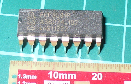
The PCF8591 is available in DIP form, which makes it easy to experiment with:

pcf8591

You can get them from the usual retailers. Before moving on, download the data sheet. The PCF8591 can operate on both 5V and 3.3V so if you’re using an Arduino Due, Raspberry Pi or other 3.3 V development board you’re fine. Now we’ll first explain the DAC, then the ADCs.

Using the DAC (digital-to-analogue converter)

The DAC on the PCF8591 has a resolution of 8-bits – so it can generate a theoretical signal of between zero volts and the reference voltage (Vref) in 255 steps. For demonstration purposes we’ll use a Vref of 5V, and you can use a lower Vref such as 3.3V or whatever you wish the maximum value to be … however it must be less than the supply voltage. Note that when there is a load on the analogue output (a real-world situation), the maximum output voltage will drop – the data sheet (which you downloaded) shows a 10% drop for a 10kΩ load. Now for our demonstration circuit:

pcf8591basic_schem

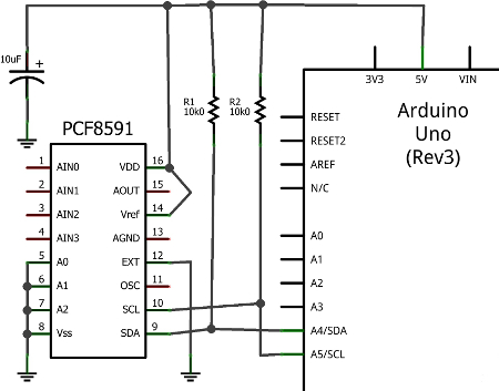
Note the use of 10kΩ pull-up resistors on the I2C bus, and the 10μF capacitor between 5V and GND. The I2C bus address is set by a combination of pins A0~A2, and with them all to GND the address is 0×90. The analogue output can be taken from pin 15 (and there’s a seperate analogue GND on pin 13. Also, connect pin 13 to GND, and circuit GND to Arduino GND.

To control the DAC we need to send two bytes of data. The first is the control byte, which simply activates the DAC and is 1000000 (or 0×40) and the next byte is the value between 0 and 255 (the output level). This is demonstrated in the following sketch (download):

// Example 52.1 PCF8591 DAC demo
// http://tronixstuff.com/tutorials Chapter 52
// John Boxall June 2013
#include "Wire.h"
#define PCF8591 (0x90 >> 1) // I2C bus address
void setup()
{
 Wire.begin();
}
void loop()
{ 
 for (int i=0; i<256; i++)
 {
 Wire.beginTransmission(PCF8591); // wake up PCF8591
 Wire.write(0x40); // control byte - turn on DAC (binary 1000000)
 Wire.write(i); // value to send to DAC
 Wire.endTransmission(); // end tranmission
 }

 for (int i=255; i>=0; --i)
 {
 Wire.beginTransmission(PCF8591); // wake up PCF8591
 Wire.write(0x40); // control byte - turn on DAC (binary 1000000)
 Wire.write(i); // value to send to DAC
 Wire.endTransmission(); // end tranmission
 }
}

Did you notice the bit shift of the bus address in the #define statement? Arduino sends 7-bit addresses but the PCF8591 wants an 8-bit, so we shift the byte over by one bit. 

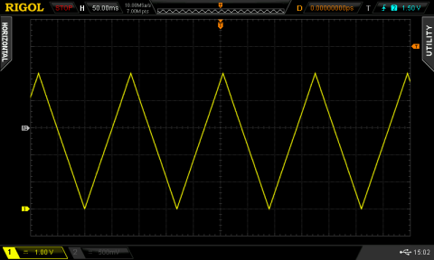
The results of the sketch are shown below, we’ve connected the Vref to 5V and the oscilloscope probe and GND to the analogue output and GND respectively (click image to enlarge):

triangle

If you like curves you can generate sine waves with the sketch below. It uses a lookup table in an array which contains the necessary pre-calculated data points (download):

// Example 52.2 PCF8591 DAC demo - sine wave
// http://tronixstuff.com/tutorials Chapter 52
// John Boxall June 2013
#include "Wire.h"
#define PCF8591 (0x90 >> 1) // I2C bus address
uint8_t sine_wave[256] = {
 0x80, 0x83, 0x86, 0x89, 0x8C, 0x90, 0x93, 0x96,
 0x99, 0x9C, 0x9F, 0xA2, 0xA5, 0xA8, 0xAB, 0xAE,
 0xB1, 0xB3, 0xB6, 0xB9, 0xBC, 0xBF, 0xC1, 0xC4,
 0xC7, 0xC9, 0xCC, 0xCE, 0xD1, 0xD3, 0xD5, 0xD8,
 0xDA, 0xDC, 0xDE, 0xE0, 0xE2, 0xE4, 0xE6, 0xE8,
 0xEA, 0xEB, 0xED, 0xEF, 0xF0, 0xF1, 0xF3, 0xF4,
 0xF5, 0xF6, 0xF8, 0xF9, 0xFA, 0xFA, 0xFB, 0xFC,
 0xFD, 0xFD, 0xFE, 0xFE, 0xFE, 0xFF, 0xFF, 0xFF,
 0xFF, 0xFF, 0xFF, 0xFF, 0xFE, 0xFE, 0xFE, 0xFD,
 0xFD, 0xFC, 0xFB, 0xFA, 0xFA, 0xF9, 0xF8, 0xF6,
 0xF5, 0xF4, 0xF3, 0xF1, 0xF0, 0xEF, 0xED, 0xEB,
 0xEA, 0xE8, 0xE6, 0xE4, 0xE2, 0xE0, 0xDE, 0xDC,
 0xDA, 0xD8, 0xD5, 0xD3, 0xD1, 0xCE, 0xCC, 0xC9,
 0xC7, 0xC4, 0xC1, 0xBF, 0xBC, 0xB9, 0xB6, 0xB3,
 0xB1, 0xAE, 0xAB, 0xA8, 0xA5, 0xA2, 0x9F, 0x9C,
 0x99, 0x96, 0x93, 0x90, 0x8C, 0x89, 0x86, 0x83,
 0x80, 0x7D, 0x7A, 0x77, 0x74, 0x70, 0x6D, 0x6A,
 0x67, 0x64, 0x61, 0x5E, 0x5B, 0x58, 0x55, 0x52,
 0x4F, 0x4D, 0x4A, 0x47, 0x44, 0x41, 0x3F, 0x3C,
 0x39, 0x37, 0x34, 0x32, 0x2F, 0x2D, 0x2B, 0x28,
 0x26, 0x24, 0x22, 0x20, 0x1E, 0x1C, 0x1A, 0x18,
 0x16, 0x15, 0x13, 0x11, 0x10, 0x0F, 0x0D, 0x0C,
 0x0B, 0x0A, 0x08, 0x07, 0x06, 0x06, 0x05, 0x04,
 0x03, 0x03, 0x02, 0x02, 0x02, 0x01, 0x01, 0x01,
 0x01, 0x01, 0x01, 0x01, 0x02, 0x02, 0x02, 0x03,
 0x03, 0x04, 0x05, 0x06, 0x06, 0x07, 0x08, 0x0A,
 0x0B, 0x0C, 0x0D, 0x0F, 0x10, 0x11, 0x13, 0x15,
 0x16, 0x18, 0x1A, 0x1C, 0x1E, 0x20, 0x22, 0x24,
 0x26, 0x28, 0x2B, 0x2D, 0x2F, 0x32, 0x34, 0x37,
 0x39, 0x3C, 0x3F, 0x41, 0x44, 0x47, 0x4A, 0x4D,
 0x4F, 0x52, 0x55, 0x58, 0x5B, 0x5E, 0x61, 0x64,
 0x67, 0x6A, 0x6D, 0x70, 0x74, 0x77, 0x7A, 0x7D
};
void setup()
{
 Wire.begin();
}
void loop()
{ 
 for (int i=0; i<256; i++)
 {
 Wire.beginTransmission(PCF8591); // wake up PCF8591
 Wire.write(0x40); // control byte - turn on DAC (binary 1000000)
 Wire.write(sine_wave[i]); // value to send to DAC
 Wire.endTransmission(); // end tranmission
 }
}

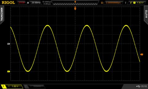
And the results (click image to enlarge):

sine

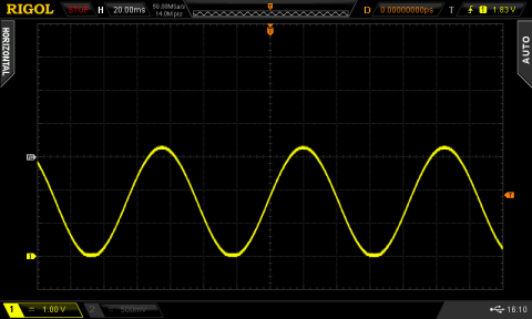
For the following DSO image dump, we changed the Vref to 3.3V – note the change in the maxima on the sine wave:

sine3v3

Now you can experiment with the DAC to make sound effects, signals or control other analogue circuits.

Using the ADCs (analogue-to-digital converters)

If you’ve used the analogRead() function on your Arduino (way back in Chapter One) then you’re already familiar with an ADC. With out PCF8591 we can read a voltage between zero and the Vref and it will return a value of between zero and 255 which is directly proportional to zero and the Vref. For example, measuring 3.3V should return 168. The resolution (8-bit) of the ADC is lower than the onboard Arduino (10-bit) however the PCF8591 can do something the Arduino’s ADC cannot. But we’ll get to that in a moment.

First, to simply read the values of each ADC pin we send a control byte to tell the PCF8591 which ADC we want to read. For ADCs zero to three the control byte is 0×00, 0×01, ox02 and 0×03 respectively. Then we ask for two bytes of data back from the ADC, and store the second byte for use. Why two bytes? The PCF8591 returns the previously measured value first – then the current byte. (See Figure 8 in the data sheet). Finally, if you’re not using all the ADC pins, connect the unused ones to GND.

The following example sketch simply retrieves values from each ADC pin one at a time, then displays them in the serial monitor (download):

// Example 52.3 PCF8591 ADC demo 
// http://tronixstuff.com/tutorials Chapter 52
// John Boxall June 2013
#include "Wire.h"
#define PCF8591 (0x90 >> 1) // I2C bus address
#define ADC0 0x00 // control bytes for reading individual ADCs
#define ADC1 0x01
#define ADC2 0x02
#define ADC3 0x03
byte value0, value1, value2, value3;
void setup()
{
 Wire.begin();
 Serial.begin(9600);
}
void loop()
{ 
 Wire.beginTransmission(PCF8591); // wake up PCF8591
 Wire.write(ADC0); // control byte - read ADC0
 Wire.endTransmission(); // end tranmission
 Wire.requestFrom(PCF8591, 2);
 value0=Wire.read();
 value0=Wire.read();
 Wire.beginTransmission(PCF8591); // wake up PCF8591
 Wire.write(ADC1); // control byte - read ADC1
 Wire.endTransmission(); // end tranmission
 Wire.requestFrom(PCF8591, 2);
 value1=Wire.read();
 value1=Wire.read();
 Wire.beginTransmission(PCF8591); // wake up PCF8591
 Wire.write(ADC2); // control byte - read ADC2
 Wire.endTransmission(); // end tranmission
 Wire.requestFrom(PCF8591, 2);
 value2=Wire.read();
 value2=Wire.read();
 Wire.beginTransmission(PCF8591); // wake up PCF8591
 Wire.write(ADC3); // control byte - read ADC3
 Wire.endTransmission(); // end tranmission
 Wire.requestFrom(PCF8591, 2);
 value3=Wire.read();
 value3=Wire.read();
 Serial.print(value0); Serial.print(" ");
 Serial.print(value1); Serial.print(" ");
 Serial.print(value2); Serial.print(" ");
 Serial.print(value3); Serial.print(" "); 
 Serial.println();
}

Upon running the sketch you’ll be presented with the values of each ADC in the serial monitor. Although it was a simple demonstration to show you how to individually read each ADC, it is a cumbersome method of getting more than one byte at a time from a particular ADC.

To do this, change the control byte to request auto-increment, which is done by setting bit 2 of the control byte to 1. So to start from ADC0 we use a new control byte of binary 00000100 or hexadecimal 0×04. Then request five bytes of data (once again we ignore the first byte) which will cause the PCF8591 to return all values in one chain of bytes. This process is demonstrated in the following sketch (download):

// Example 52.4 PCF8591 ADC demo 
// http://tronixstuff.com/tutorials Chapter 52
// John Boxall June 2013
#include "Wire.h"
#define PCF8591 (0x90 >> 1) // I2C bus address
byte value0, value1, value2, value3;
void setup()
{
 Wire.begin();
 Serial.begin(9600);
}
void loop()
{ 
 Wire.beginTransmission(PCF8591); // wake up PCF8591
 Wire.write(0x04); // control byte - read ADC0 then auto-increment
 Wire.endTransmission(); // end tranmission
 Wire.requestFrom(PCF8591, 5); 
 value0=Wire.read();
 value0=Wire.read(); 
 value1=Wire.read(); 
 value2=Wire.read(); 
 value3=Wire.read();
 Serial.print(value0); Serial.print(" ");
 Serial.print(value1); Serial.print(" ");
 Serial.print(value2); Serial.print(" ");
 Serial.print(value3); Serial.print(" "); 
 Serial.println();
}

Previously we mentioned that the PCF8591 can do something that the Arduino’s ADC cannot, and this is offer a differential ADC. As opposed to the Arduino’s single-ended (i.e. it returns the difference between the positive signal voltage and GND, the differential ADC accepts two signals (that don’t necessarily have to be referenced to ground), and returns the difference between the two signals. This can be convenient for measuring small changes in voltages for load cells and so on.

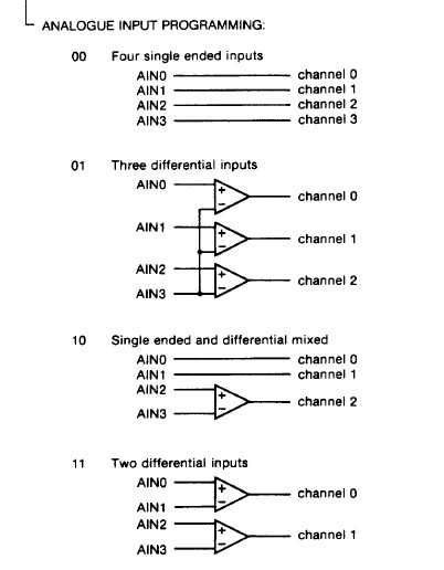
Setting up the PCF8591 for differential ADC is a simple matter of changing the control byte. If you turn to page seven of the data sheet, then consider the different types of analogue input programming. Previously we used mode ’00′ for four inputs, however you can select the others which are clearly illustrated, for example:

adcmodes

So to set the control byte for two differential inputs, use binary 00110000 or 0×30. Then it’s a simple matter of requesting the bytes of data and working with them. As you can see there’s also combination single/differential and a complex three-differential input. However we’ll leave them for the time being.

Conclusion

Hopefully you found this of interest, whether adding a DAC to your experiments or learning a bit more about ADCs. We’ll have some more analogue to digital articles coming up soon, so stay tuned. And if you enjoy my tutorials, or want to introduce someone else to the interesting world of Arduino – check out my new book “Arduino Workshop” from No Starch Press.

In the meanwhile have fun and keep checking into tronixstuff.com. Why not follow things on twitterGoogle+, subscribe  for email updates or RSS using the links on the right-hand column? And join our friendly Google Group – dedicated to the projects and related items on this website. Sign up – it’s free, helpful to each other –  and we can all learn something.


Learn how to use the NXP PCF 8591 8-bit A/D and D/A IC with Arduino in chapter fifty-two of my Arduino Tutorials. The first chapter is here, the complete series is detailed here.

Updated 17/06/2013

Introduction

Have you ever wanted more analogue input pins on your Arduino project, but not wanted to fork out for a Mega? Or would you like to generate analogue signals? Then check out the subject of our tutorial – the NXP PCF8591 IC. It solves both these problems as it has a single DAC (digital to analogue) converter as well as four ADCs (analogue to digital converters) – all accessible via the I2C bus. If the I2C bus is new to you, please familiarise yourself with the readings here before moving forward.

The PCF8591 is available in DIP form, which makes it easy to experiment with:

pcf8591

You can get them from the usual retailers. Before moving on, download the data sheet. The PCF8591 can operate on both 5V and 3.3V so if you’re using an Arduino Due, Raspberry Pi or other 3.3 V development board you’re fine. Now we’ll first explain the DAC, then the ADCs.

Using the DAC (digital-to-analogue converter)

The DAC on the PCF8591 has a resolution of 8-bits – so it can generate a theoretical signal of between zero volts and the reference voltage (Vref) in 255 steps. For demonstration purposes we’ll use a Vref of 5V, and you can use a lower Vref such as 3.3V or whatever you wish the maximum value to be … however it must be less than the supply voltage. Note that when there is a load on the analogue output (a real-world situation), the maximum output voltage will drop – the data sheet (which you downloaded) shows a 10% drop for a 10kΩ load. Now for our demonstration circuit:

pcf8591basic_schem

Note the use of 10kΩ pull-up resistors on the I2C bus, and the 10μF capacitor between 5V and GND. The I2C bus address is set by a combination of pins A0~A2, and with them all to GND the address is 0×90. The analogue output can be taken from pin 15 (and there’s a seperate analogue GND on pin 13. Also, connect pin 13 to GND, and circuit GND to Arduino GND.

To control the DAC we need to send two bytes of data. The first is the control byte, which simply activates the DAC and is 1000000 (or 0×40) and the next byte is the value between 0 and 255 (the output level). This is demonstrated in the following sketch:

// Example 52.1 PCF8591 DAC demo
// http://tronixstuff.com/tutorials Chapter 52
// John Boxall June 2013
#include "Wire.h"
#define PCF8591 (0x90 >> 1) // I2C bus address
void setup()
{
 Wire.begin();
}
void loop()
{
 for (int i=0; i<256; i++)
 {
 Wire.beginTransmission(PCF8591); // wake up PCF8591
 Wire.write(0x40); // control byte - turn on DAC (binary 1000000)
 Wire.write(i); // value to send to DAC
 Wire.endTransmission(); // end tranmission
 }

 for (int i=255; i>=0; --i)
 {
 Wire.beginTransmission(PCF8591); // wake up PCF8591
 Wire.write(0x40); // control byte - turn on DAC (binary 1000000)
 Wire.write(i); // value to send to DAC
 Wire.endTransmission(); // end tranmission
 }
}

Did you notice the bit shift of the bus address in the #define statement? Arduino sends 7-bit addresses but the PCF8591 wants an 8-bit, so we shift the byte over by one bit. 

The results of the sketch are shown below, we’ve connected the Vref to 5V and the oscilloscope probe and GND to the analogue output and GND respectively:

triangle

If you like curves you can generate sine waves with the sketch below. It uses a lookup table in an array which contains the necessary pre-calculated data points:

// Example 52.2 PCF8591 DAC demo - sine wave
// http://tronixstuff.com/tutorials Chapter 52
// John Boxall June 2013

#include "Wire.h"
#define PCF8591 (0x90 >> 1) // I2C bus address

uint8_t sine_wave[256] = {
 0x80, 0x83, 0x86, 0x89, 0x8C, 0x90, 0x93, 0x96,
 0x99, 0x9C, 0x9F, 0xA2, 0xA5, 0xA8, 0xAB, 0xAE,
 0xB1, 0xB3, 0xB6, 0xB9, 0xBC, 0xBF, 0xC1, 0xC4,
 0xC7, 0xC9, 0xCC, 0xCE, 0xD1, 0xD3, 0xD5, 0xD8,
 0xDA, 0xDC, 0xDE, 0xE0, 0xE2, 0xE4, 0xE6, 0xE8,
 0xEA, 0xEB, 0xED, 0xEF, 0xF0, 0xF1, 0xF3, 0xF4,
 0xF5, 0xF6, 0xF8, 0xF9, 0xFA, 0xFA, 0xFB, 0xFC,
 0xFD, 0xFD, 0xFE, 0xFE, 0xFE, 0xFF, 0xFF, 0xFF,
 0xFF, 0xFF, 0xFF, 0xFF, 0xFE, 0xFE, 0xFE, 0xFD,
 0xFD, 0xFC, 0xFB, 0xFA, 0xFA, 0xF9, 0xF8, 0xF6,
 0xF5, 0xF4, 0xF3, 0xF1, 0xF0, 0xEF, 0xED, 0xEB,
 0xEA, 0xE8, 0xE6, 0xE4, 0xE2, 0xE0, 0xDE, 0xDC,
 0xDA, 0xD8, 0xD5, 0xD3, 0xD1, 0xCE, 0xCC, 0xC9,
 0xC7, 0xC4, 0xC1, 0xBF, 0xBC, 0xB9, 0xB6, 0xB3,
 0xB1, 0xAE, 0xAB, 0xA8, 0xA5, 0xA2, 0x9F, 0x9C,
 0x99, 0x96, 0x93, 0x90, 0x8C, 0x89, 0x86, 0x83,
 0x80, 0x7D, 0x7A, 0x77, 0x74, 0x70, 0x6D, 0x6A,
 0x67, 0x64, 0x61, 0x5E, 0x5B, 0x58, 0x55, 0x52,
 0x4F, 0x4D, 0x4A, 0x47, 0x44, 0x41, 0x3F, 0x3C,
 0x39, 0x37, 0x34, 0x32, 0x2F, 0x2D, 0x2B, 0x28,
 0x26, 0x24, 0x22, 0x20, 0x1E, 0x1C, 0x1A, 0x18,
 0x16, 0x15, 0x13, 0x11, 0x10, 0x0F, 0x0D, 0x0C,
 0x0B, 0x0A, 0x08, 0x07, 0x06, 0x06, 0x05, 0x04,
 0x03, 0x03, 0x02, 0x02, 0x02, 0x01, 0x01, 0x01,
 0x01, 0x01, 0x01, 0x01, 0x02, 0x02, 0x02, 0x03,
 0x03, 0x04, 0x05, 0x06, 0x06, 0x07, 0x08, 0x0A,
 0x0B, 0x0C, 0x0D, 0x0F, 0x10, 0x11, 0x13, 0x15,
 0x16, 0x18, 0x1A, 0x1C, 0x1E, 0x20, 0x22, 0x24,
 0x26, 0x28, 0x2B, 0x2D, 0x2F, 0x32, 0x34, 0x37,
 0x39, 0x3C, 0x3F, 0x41, 0x44, 0x47, 0x4A, 0x4D,
 0x4F, 0x52, 0x55, 0x58, 0x5B, 0x5E, 0x61, 0x64,
 0x67, 0x6A, 0x6D, 0x70, 0x74, 0x77, 0x7A, 0x7D
};
void setup()
{
 Wire.begin();
}
void loop()
{
 for (int i=0; i<256; i++)
 {
 Wire.beginTransmission(PCF8591); // wake up PCF8591
 Wire.write(0x40); // control byte - turn on DAC (binary 1000000)
 Wire.write(sine_wave[i]); // value to send to DAC
 Wire.endTransmission(); // end tranmission
 }
}

And the results:

sine

For the following DSO image dump, we changed the Vref to 3.3V – note the change in the maxima on the sine wave:

sine3v3

Now you can experiment with the DAC to make sound effects, signals or control other analogue circuits.

Using the ADCs (analogue-to-digital converters)

If you’ve used the analogRead() function on your Arduino (way back in Chapter One) then you’re already familiar with an ADC. With out PCF8591 we can read a voltage between zero and the Vref and it will return a value of between zero and 255 which is directly proportional to zero and the Vref. For example, measuring 3.3V should return 168. The resolution (8-bit) of the ADC is lower than the onboard Arduino (10-bit) however the PCF8591 can do something the Arduino’s ADC cannot. But we’ll get to that in a moment.

First, to simply read the values of each ADC pin we send a control byte to tell the PCF8591 which ADC we want to read. For ADCs zero to three the control byte is 0×00, 0×01, ox02 and 0×03 respectively. Then we ask for two bytes of data back from the ADC, and store the second byte for use. Why two bytes? The PCF8591 returns the previously measured value first – then the current byte. (See Figure 8 in the data sheet). Finally, if you’re not using all the ADC pins, connect the unused ones to GND.

The following example sketch simply retrieves values from each ADC pin one at a time, then displays them in the serial monitor:

// Example 52.3 PCF8591 ADC demo
// http://tronixstuff.com/tutorials Chapter 52
// John Boxall June 2013
#include "Wire.h"
#define PCF8591 (0x90 >> 1) // I2C bus address
#define ADC0 0x00 // control bytes for reading individual ADCs
#define ADC1 0x01
#define ADC2 0x02
#define ADC3 0x03
byte value0, value1, value2, value3;
void setup()
{
 Wire.begin();
 Serial.begin(9600);
}
void loop()
{
 Wire.beginTransmission(PCF8591); // wake up PCF8591
 Wire.write(ADC0); // control byte - read ADC0
 Wire.endTransmission(); // end tranmission
 Wire.requestFrom(PCF8591, 2);
 value0=Wire.read();
 value0=Wire.read();
 Wire.beginTransmission(PCF8591); // wake up PCF8591
 Wire.write(ADC1); // control byte - read ADC1
 Wire.endTransmission(); // end tranmission
 Wire.requestFrom(PCF8591, 2);
 value1=Wire.read();
 value1=Wire.read();
 Wire.beginTransmission(PCF8591); // wake up PCF8591
 Wire.write(ADC2); // control byte - read ADC2
 Wire.endTransmission(); // end tranmission
 Wire.requestFrom(PCF8591, 2);
 value2=Wire.read();
 value2=Wire.read();
 Wire.beginTransmission(PCF8591); // wake up PCF8591
 Wire.write(ADC3); // control byte - read ADC3
 Wire.endTransmission(); // end tranmission
 Wire.requestFrom(PCF8591, 2);
 value3=Wire.read();
 value3=Wire.read();
 Serial.print(value0); Serial.print(" ");
 Serial.print(value1); Serial.print(" ");
 Serial.print(value2); Serial.print(" ");
 Serial.print(value3); Serial.print(" ");
 Serial.println();
}

Upon running the sketch you’ll be presented with the values of each ADC in the serial monitor. Although it was a simple demonstration to show you how to individually read each ADC, it is a cumbersome method of getting more than one byte at a time from a particular ADC.

To do this, change the control byte to request auto-increment, which is done by setting bit 2 of the control byte to 1. So to start from ADC0 we use a new control byte of binary 00000100 or hexadecimal 0×04. Then request five bytes of data (once again we ignore the first byte) which will cause the PCF8591 to return all values in one chain of bytes. This process is demonstrated in the following sketch:

// Example 52.4 PCF8591 ADC demo
// http://tronixstuff.com/tutorials Chapter 52
// John Boxall June 2013
#include "Wire.h"
#define PCF8591 (0x90 >> 1) // I2C bus address
byte value0, value1, value2, value3;
void setup()
{
 Wire.begin();
 Serial.begin(9600);
}
void loop()
{
 Wire.beginTransmission(PCF8591); // wake up PCF8591
 Wire.write(0x04); // control byte - read ADC0 then auto-increment
 Wire.endTransmission(); // end tranmission
 Wire.requestFrom(PCF8591, 5);
 value0=Wire.read();
 value0=Wire.read();
 value1=Wire.read();
 value2=Wire.read();
 value3=Wire.read();
 Serial.print(value0); Serial.print(" ");
 Serial.print(value1); Serial.print(" ");
 Serial.print(value2); Serial.print(" ");
 Serial.print(value3); Serial.print(" ");
 Serial.println();
}

Previously we mentioned that the PCF8591 can do something that the Arduino’s ADC cannot, and this is offer a differential ADC. As opposed to the Arduino’s single-ended (i.e. it returns the difference between the positive signal voltage and GND, the differential ADC accepts two signals (that don’t necessarily have to be referenced to ground), and returns the difference between the two signals. This can be convenient for measuring small changes in voltages for load cells and so on.

Setting up the PCF8591 for differential ADC is a simple matter of changing the control byte. If you turn to page seven of the data sheet, then consider the different types of analogue input programming. Previously we used mode ’00′ for four inputs, however you can select the others which are clearly illustrated, for example:

adcmodes

So to set the control byte for two differential inputs, use binary 00110000 or 0×30. Then it’s a simple matter of requesting the bytes of data and working with them. As you can see there’s also combination single/differential and a complex three-differential input. However we’ll leave them for the time being.

Conclusion

Hopefully you found this of interest, whether adding a DAC to your experiments or learning a bit more about ADCs. We’ll have some more analogue to digital articles coming up soon, so stay tuned. And if you enjoy my tutorials, or want to introduce someone else to the interesting world of Arduino – check out my new book “Arduino Workshop” from No Starch Press.

LEDborder

In the meanwhile have fun and keep checking into tronixstuff.com. Why not follow things on twitterGoogle+, subscribe  for email updates or RSS using the links on the right-hand column? And join our friendly Google Group – dedicated to the projects and related items on this website. Sign up – it’s free, helpful to each other –  and we can all learn something.
The post Tutorial – Arduino and PCF8591 ADC DAC IC appeared first on tronixstuff.

Hello readers

Today we continue down the path of analog electronics theory by stopping by for an introductory look at the RC circuit. That’s R for resistor, and C for capacitor. As we know from previous articles, resistors can resist or limit the flow of current in a circuit, and a capacitor stores electric current for use in the future. And – when used together – these two simple components can be used for many interesting applications such as timing and creating oscillators of various frequencies.

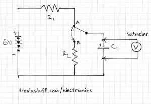
How is this so? Please consider the following simple circuit:

When the switch is in position A, current flows through R1 and into the capacitor C1 until it is fully charged. During this charging process, the voltage across the capacitor will change, starting from zero until fully charged, at which point the voltage will be the same as if the capacitor had been replaced by a break in the circuit – in this case 6V. Fair enough. But how long will the capacitor take to reach this state? Well the time taken is a function of several things – including the value of the resistor (R1) as it limits the flow of current; and the size of the capacitor – which determines how much charge can be stored.

If we know these two values, we can calculate the time constant of the circuit. The time constant is denoted by the character zeta (lower-case Greek Z).

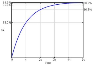
The time constant is the time taken (in seconds) by the capacitor C that is fed from a resistor R to charge to a certain level. The capacitor will charge to 63% of the final voltage in one time constant, 85% in two time constants, and 100% in five time constants. If you graphed the % charge against time constant, the result is exponential. That is:

Now enough theory – let’s put this RC circuit to practice to see the voltage change across the capacitor as it charges. The resistor R1 will be 20k ohm, the capacitor 1000 uF.

Our time constant will be R x C which will be 20000 ohms x 0.001 farads, which equals 20 (seconds).  Notice the unit conversion – you need to go back to ohms and farads not micro-, pico- or nanofarads. So our example will take 20 seconds to reach 63% of final voltage, and 100 seconds to reach almost full voltage. This is assuming the values of the resistor and capacitor are accurate. The capacitor will have to be taken on face value as I can’t measure it with my equipment, and don’t have the data sheet to know the tolerance. The resistor measured at 19.84 k ohms, and the battery measured 6.27 volts. Therefore our real time constant should be around 19.84 seconds, give or take.

First of all, here is a shot of the little oscilloscope measuring the change in voltage over the capacitor with respect to time. The vertical scale is 1v/division:

And here is the multimeter measuring the voltage next to a stopwatch. (crude yet effective, no?)

The two videos were not the most accurate, as it was difficult to synchronise the stopwatch and start the circuit, but I hope you could see the exponential relationship between time and voltage.

What about discharging? Using the circuit above, if we moved the switch to B after charging the capacitor –  and R2 was also 20k ohm – how long would it take to discharge the capacitor? Exactly the same as charging it! So one time constant to discharge 63% and so on. So you can take the graph from above and invert it as such:

How can we make use of an RC circuit?

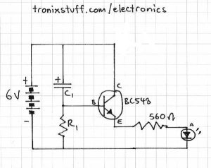
I’m glad you asked. Consider the following circuit:

When power is applied, the capacitor starts to charge, and in doing so allows current to flow to the emitter of the transistor, which turns on the LED. However as the capacitor charges, less current passes to the base of the transistor, eventually turning it off. Therefore you can calculate time constants and experiment to create an off timer. However, a preferable way would be to make use of a 555 timer. For example, an RC combination is used to set the pulse length used in astable timing applications, for example using R1, R2 and C1:

(For more information on the 555 timer, please read this article)

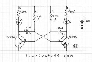
Another use of the RC circuit is oscillating. Due to varying capacitor values due to tolerance, you most likely cannot make precision frequency generators, but you can still have some fun and make useful things. Here is a classic oscillator example – an astable multivibrator:

What is going on here? Here it is in action:

and here is one side being measured on the little scope:

We have two RC circuits, each controlling a transistor. When power is applied, there is no way to determine which side will start first, as this depends on the latent charge in the capacitors and the exact values of the resistors and capacitors. So to start let’s assume the left transistor (Q1) and LED are on; and the right transistor (Q2) and LED are off. The voltage at collector of Q1 will be close to zero as it is on. And the voltage at the base of Q2 will also be close to zero as C2 will initially be discharged. But C2 will now start charging via R4 and base of Q1 to around 5.4V (remember the 0.6v loss over the base-emitter junction of a transistor). While this is happening, C1 starts charging through R2. Once the voltage difference reaches 0.6V over the capacitor, Q2 is turned on.

But when Q2 is on, the voltage at the collector drops to zero, and C2 is charged, so it pulls the voltage at the base of Q1 to -5.4v, turning it off and the left LED. C1 starts charging via R1, and C2 starts charging via R3 until it reaches 0.6v. Then Q1 turns on, bringing the base of Q2 down to -5.4V – switching it off. And the whole process repeats itself. Argh. Now you can see why Arduino is so popular.

Time for a laugh – here is the result of too much current through a trimpot:

So there you have it – the RC circuit. Part of the magic of analogue electronics!

As always, thank you for reading and I look forward to your comments and so on. Furthermore, don’t be shy in pointing out errors or places that could use improvement. Please subscribe using one of the methods at the top-right of this web page to receive updates on new posts. Or join our new Google Group.

Otherwise, have fun, be good to each other – and make something! :)


  • Newsletter

    Sign up for the PlanetArduino Newsletter, which delivers the most popular articles via e-mail to your inbox every week. Just fill in the information below and submit.

  • Like Us on Facebook