Posts | Comments

Planet Arduino

Archive for the ‘silicon’ Category

Introduction

Every month Australian electronics magazine Silicon Chip publishes a variety of projects, and in February 1994 they published the “90 Second Digital Message Recorder” project. That was a long time ago, however you can still find the kit today at Altronics (and at the time of writing, on sale for AU$26), and thus the subject of our review.

The kit offers a simple method of recording and playing back 90 seconds of audio, captured with an electret microphone. When mounted in a suitable enclosure it will make a neat way of leaving messages or instructions for others at home.

Assembly

The kit arrives in typical Altronics fashion:

Altronics K9570 90 second message recorder kit package

… and includes everything required including IC sockets for the ISD2590 and the audio amplifier:

Altronics K9570 90 second message recorder kit inclusions

Altronics K9570 90 second message recorder kit components

The PCB missed out on silk-screening – which is a pity:

Altronics K9570 90 second message recorder kit instructions PCB front

however it is from an original design from twenty years ago. The solder mask is neat and helps prevent against lazy soldering mistakes:

Altronics K9570 90 second message recorder kit PCB back

Finally the detailed instructions including component layout and the handy Altronics reference guide are also included. After checking and ordering the resistors, they were installed first along with the links:

Altronics K9570 90 second message recorder kit construction

 If you have your own kit, there is a small error in the instructions. The resistor between the 2k2 and the 10uF electrolytic at the top of the board is 10k0 not 2k2. Moving on, these followed by the capacitors and other low-profile components:

Altronics K9570 90 second message recorder kit construction 4

The rest of the components went in without any fuss, and frankly it’s a very easy kit to assemble:

Altronics K9570 90 second message recorder kit finished

 The required power supply is 6V, and a power switch and 4 x AA cell holder is included however were omitted for the review.

How it works

Instead of some fancy microcontrollers, the kit uses an ISD2590P single chip voice recording and playback IC:

Altronics K9570 90 second message recorder kit ISD2590

It’s a neat part that takes care of most of the required functions including microphone preamp, automatic gain control, and an EEPROM to store the analogue voltage levels that make up the voice sample. The ISD2590 samples audio at 5.3 kHz which isn’t CD quality, but enough for its intended purpose.

Apart from some passive components for power filtering, controls and a speaker amplifier there isn’t much else to say. Download the ISD2590 data sheet (pdf), which is incredibly detailed including some example circuits.

Operation

Once you apply power it’s a simple matter of setting the toggle switch on the PCB down for record, or up for playback. You can record in more than one session, and each session is recorded in order until the memory is full. Then the sounds can be played back without any fuss.

The kit is supplied with the generic 0.25W speaker which is perhaps a little weak for the amplifier circuit in the kit, however by turning down the volume a little the sound is adequate. In this video you can see (and hear) a quick recording and playback session.

Conclusion

This kit could be the base for convenient message system – and much more interesting than just scribbling notes for each other. Or you could built it into a toy and have it play various tunes or speech to amuse children. And for the price it’s great value to experiment with an ISD2590 – just use an IC socket. Or just have some fun  – we did.  Full-sized images are available on flickr

And if you enjoyed this article, or want to introduce someone else to the interesting world of Arduino – check out my book (now in a third printing!) “Arduino Workshop”.

visit tronixlabs.com

Have fun and keep checking into tronixstuff.com. Why not follow things on twitterGoogle+, subscribe  for email updates or RSS using the links on the right-hand column, or join our forum – dedicated to the projects and related items on this website. Sign up – it’s free, helpful to each other –  and we can all learn something.
Nov
10

Introduction

In this review of an older kit (circa 1993~1997) we examine the Diesel Sound Simulator for Model Railroads kit from (the now defunct) Dick Smith Electronics, based on the article published in the December 1992 issue of Silicon Chip magazine.

The purpose of this kit is to give you a small circuit which can fit in a HO scale (or larger) locomotive, or hidden underneath the layout – that can emulate the rumbling of a diesel-electric locomotive to increase the realism of a train. However the kit is designed for use with a PWM train controller (also devised by Silicon Chip!) so not for the simple direct-DC drive layouts.

K3030 diesel sound simulator kit

Assembly

The diesel sound kit was from the time when DSE still cared about kits, so you received the sixteen page “Guide to Kit Construction” plus the kit instructions, nasty red disclaimer sheet, feedback card, plus all the required components and the obligatory coil of solder that was usually rubbish:

K3030 diesel sound simulator kit contents

Everything required to get going is included, except IC sockets. My theory is it’s cheaper to use your own sockets than source older CMOS/TTL later on if you want to reuse the ICs, so sockets are now mandatory here:

K3030 diesel sound simulator kit parts

The PCB is from the old school of “figure-it-out-yourself”, no fancy silk-screening here:

K3030 diesel sound simulator kit PCB

K3030 diesel sound simulator kit PCB bottom

Notice the five horizontal pads between the two ICs – these were for wire bridges in case you needed to break the PCB in two to fit inside your locomotive.

Actual assembly was straight-forward, all the components went in without any issues. Having two links under IC2 was a little annoying, however a short while later the PCB was finished and the speaker attached:

K3030 diesel sound simulator kit finished

How it works

As mentioned earlier this diesel sound kit was designed for use with the Silicon Chip train PWM controller, so the design is a little different than expected. It can handle a voltage of around 20 V, and the sound is determined by the speed of the locomotive.

The speed is determined by the back EMF measured from the motor – and (from the manual) this is the voltage produced by the motor which opposes the current flow through it and this voltage is directly proportional to speed.

Not having a 20V DC PWM supply laying about I knocked up an Arduino to PWM a 20V DC supply via an N-MOSFET module and experimented with the duty cycle to see what sort of noises could be possible. The output was affected somewhat by the supply voltage, however seemed a little higher in pitch than expected.

You can listen to the results in the following video:

I reckon the sound from around the twenty second mark isn’t a bad idle noise, however in general not that great. The results will ultimately be a function of a lower duty-cycle than I could create at the time and the values of R1 and R2 used in the kit.

 Conclusion

Another kit review over. With some time spent experimenting you could generate the required diesel sounds, a Paxman-Valenta it isn’t… but it was a fun kit and I’m sure it was well-received at the time. To those who have been asking me privately, no I don’t have a secret line to some underground warehouse of old kits – just keep an eye out on ebay and they pop up now and again. Full-sized images and much more information about the kit are available on flickr.

And while you’re here – are you interested in Arduino? Check out my new book “Arduino Workshop” from No Starch Press.

In the meanwhile have fun and keep checking into tronixstuff.com. Why not follow things on twitterGoogle+, subscribe  for email updates or RSS using the links on the right-hand column? And join our friendly Google Group – dedicated to the projects and related items on this website. Sign up – it’s free, helpful to each other –  and we can all learn something.

The post Old Kit Review – Diesel Sound Simulator for Model Railroads appeared first on tronixstuff.

Introduction

Every month Australian electronics magazine Silicon Chip publishes a few projects, and in this kit review we’ll look at an older but still current example from August 2004 – the 3-state Logic Probe Kit (Mk II). This is an inexpensive piece of test equipment that’s useful when checking digital logic states and as a kit, great for beginners. Avid readers of my kit reviews may remember the SMD version we examined in June… well it wasn’t that much of a success due to the size of the parts. However this through-hole version has been quite successful, so keep reading to find out more

Assembly

The kit is packaged in typical form, without any surprises:

bag

 In typical Altronics fashion, an updated assembly guide is provided along with a general reference to common electronics topics:

bagcontents

 All the required parts are included – except for a 14-pin IC socket and two CR2016 batteries.

parts

 The PCB makes soldering easy with the silk-screen and solder mask:

pcbtop

 However the resistor numbering is a bit out of whack, a few R-numbers are skipped. So before soldering, measure and line up all the resistors in numbered order – doing so will reduce the chance of fitting them in the wrong spot.

pcbbottom

When it comes time to solder the power switch on the end, it’s necessary to clip off two tabs – one at each end of the switch. However this isn’t a problem:

solderswitchon

Soldering in the rest of the components wasn’t any effort at all, they’ve been spaced around the PCB nicely:

gettingthere

 Once they’re in, it’s time to insert the pins that hold the probe (shown on the left below):

pinsforprobe

 A full-sized probe is included with the kit, which you cut down with a hacksaw to allow it to fit on the end of the PCB. Then solder a short wire from the tip’s collar and run it through the body as such:

pinsforprobe2

 At this point, it’s time to break out the butane torch:

blowtorch

… with which you melt down the heatshrink over the tip, then fit it to the PCB and solder the probe wire:

testing

At this point it’s wise to fit the batteries and test that the probe works, as the next stage is to heatshrink the entire circuit to the left of the LEDs:

finished

Use

Using the probe is incredibly simple – however note that it’s designed for working with 5V logic. If you need to use higher voltages the probe can be assembled with slightly different circuit to take care of that eventuality. Moving forward simply clip the lead to GND on the circuit under test, then probe where you want to measure. The LEDs will indicate either HIGH, LOW or the PULSE LED will light when a fault is apparent, or other need for further research into the circuit. Here’s a quick demonstration probing a signal from an Arduino board:

Conclusion

This through-hole version of the logic probe kit was much easier to construct than the SMD version, and worked first time. A logic probe itself is a very useful tool to have and I highly recommend this kit for the beginner who enjoys projects and is growing their stable of test equipment on a budget. You can find the kit at Altronics and their distributors.

Full-sized images available on flickr.  And if you made it this far – check out my new book “Arduino Workshop” from No Starch Press.

In the meanwhile have fun and keep checking into tronixstuff.com. Why not follow things on twitterGoogle+, subscribe  for email updates or RSS using the links on the right-hand column? And join our friendly Google Group – dedicated to the projects and related items on this website. Sign up – it’s free, helpful to each other –  and we can all learn something.

[Note - kit purchased without notifying the supplier]

The post Kit review – Altronics Logic Probe Mk II appeared first on tronixstuff.

Introduction

Every month Australian electronics magazine Silicon Chip publishes a variety of projects, and in March 2004  they published the “DC-DC converter” project. Altronics picked it up and now offers a kit, the subject of our review. The main purpose of this converter kit is to allow replacement of expensive PP3 9V batteries with 2 AA cells, to enable a cheaper and longer lifespan over use. With a slight modification it can also act as a trickle-charger for 2 rechargeable AA cells (that can then supply power to the converter) via a plugpack. And there’s some educational value if you’re so inclined, as you can learn about voltage converters as well.

Assembly

As usual for Altronics the kit is in a typical retail package:

packaged

…which includes the detailed instructions (based on the original Silicon Chip article), a handy reference guide and of course the parts:

contents

The PCB has a good silk screen and solder mask:

pcbtop

pcbbottom

and all the required parts are included:

components

It was nice to see plenty of extra black and red wire for modifications or final installations, the battery snap, 2 x AA cell holder and a DC socket for use with the optional plug pack mentioned earlier. That hand-wound inductor was interesting, and I couldn’t help but measure it on the LC meter:

lcmeter

It was supposed to be a 47 uH inductor, so let’s hope that doesn’t cause too much trouble. Assembly was quite straight-forward – just start with the smallest components first and build up. If you’re not going to have the trickle-charge function, heed the notes in the manual and don’t install D2 or R4. The only fiddly bit was the “short as possible” (red) link across the board:

longlink

And after a few more minutes it was finished. The external connections will vary depending on your application – however for the review I’ve got the 9V snap on the input, which makes it easy to connect the 2 AA cell holder to power the converter. Nice to see the holes around the perimeter of the board, which make mounting it more permanently quite easy.

Operation

After a bench clean-up it was time to connect 2 AA rechargeable cells and see what we can get out of the converter. The cells measured 2.77V together before connection, and without a load on the converter the resulting output was 8.825 V:

firsttest

We can live with that. Furthermore the quiescent current (a situation with the power connected and not having a load on the output) was 2.5 mA. Thus it would be a good idea to have a power switch in a real-world environment. Speaking of the real world (!) how much current can you get out of the converter? Generally PP3 battery applications are low current, as the battery itself isn’t good for that much – even an expensive “Energizer Ultimate Lithium” offers only 800 mAh (for $16). So using higher-capacity rechargeable AA cells and this kit will save money.  A table is included with the instructions that shows the possible uses:

tableofuse

According to the table my 2.77V supply should be good for ~80 mA. With some resistors in parallel we made a dummy load of 69 mA and measured 0.37A current draw from the AA cells. Thus the key to this kit – you find a cheaper or more plentiful power supply at a lower voltage to save you the expense of providing the higher voltage.

For example, if you had a pair of Sanyo Eneloop rechargeable AA cells (total 2.4 V at 2 Ah) they would give you around 5.4 hours of life (ignoring the fall-off of voltage towards the end of their charge life – however the eneloops are pretty good in that regard). Whereas a disposable PP3 mentioned earlier would offer around 2.1 hours (at $16) or a rechargeable unit (which offers 8.4 V at 175 mAh) would only last around 25 minutes. Note that you can change two resistors in the circuit to alter the output voltage, and the values have been listed in the instructions for outputs up to 15 V.

Finally, let’s consider the output waveforms from the circuit. With the aforementioned load, here’s the output on the DSO (click image to enlarge):

output

… and for interest’s sake, the switching output from the TL499 (click images to enlarge):

switchoutput

switchoutputdata

Conclusion

Apart from the described voltage-boosting functions this kit gives the interested builder experience with boost circuits and also the knowledge to create their own versions based on the original design, at a much lower cost than using other boost ICs . If you wanted a permanent certain voltage output, it would be better to breadboard the kit and experiment with the required resistors – then assemble the kit with the new values. And there is money and effort to be saved when subsituting with PP3 batteries. Finally, learning is a good thing!

So – a lot of fun and education for under $20. Purchase it from Altronics and their resellers, or read more about it in the September 2007 edition of Silicon Chip.

Full-sized images available on flickr. This kit was purchased without notifying the supplier.

And if you made it this far – check out my new book “Arduino Workshop” from No Starch Press.

In the meanwhile have fun and keep checking into tronixstuff.com. Why not follow things on twitterGoogle+, subscribe  for email updates or RSS using the links on the right-hand column? And join our friendly Google Group – dedicated to the projects and related items on this website. Sign up – it’s free, helpful to each other –  and we can all learn something.


Introduction

Every month Australian electronics magazine Silicon Chip publishes a variety of projects, and in March 2004  they published the “DC-DC converter” project. Altronics picked it up and now offers a kit, the subject of our review. The main purpose of this converter kit is to allow replacement of expensive PP3 9V batteries with 2 AA cells, to enable a cheaper and longer lifespan over use. With a slight modification it can also act as a trickle-charger for 2 rechargeable AA cells (that can then supply power to the converter) via a plugpack. And there’s some educational value if you’re so inclined, as you can learn about voltage converters as well.

Assembly

As usual for Altronics the kit is in a typical retail package:

packaged

…which includes the detailed instructions (based on the original Silicon Chip article), a handy reference guide and of course the parts:

contents

The PCB has a good silk screen and solder mask:

pcbtop

pcbbottom

and all the required parts are included:

components

It was nice to see plenty of extra black and red wire for modifications or final installations, the battery snap, 2 x AA cell holder and a DC socket for use with the optional plug pack mentioned earlier. That hand-wound inductor was interesting, and I couldn’t help but measure it on the LC meter:

lcmeter

It was supposed to be a 47 uH inductor, so let’s hope that doesn’t cause too much trouble. Assembly was quite straight-forward – just start with the smallest components first and build up. If you’re not going to have the trickle-charge function, heed the notes in the manual and don’t install D2 or R4. The only fiddly bit was the “short as possible” (red) link across the board:

longlink

And after a few more minutes it was finished. The external connections will vary depending on your application – however for the review I’ve got the 9V snap on the input, which makes it easy to connect the 2 AA cell holder to power the converter. Nice to see the holes around the perimeter of the board, which make mounting it more permanently quite easy.

Operation

After a bench clean-up it was time to connect 2 AA rechargeable cells and see what we can get out of the converter. The cells measured 2.77V together before connection, and without a load on the converter the resulting output was 8.825 V:

firsttest

We can live with that. Furthermore the quiescent current (a situation with the power connected and not having a load on the output) was 2.5 mA. Thus it would be a good idea to have a power switch in a real-world environment. Speaking of the real world (!) how much current can you get out of the converter? Generally PP3 battery applications are low current, as the battery itself isn’t good for that much – even an expensive “Energizer Ultimate Lithium” offers only 800 mAh (for $16). So using higher-capacity rechargeable AA cells and this kit will save money.  A table is included with the instructions that shows the possible uses:

tableofuse

According to the table my 2.77V supply should be good for ~80 mA. With some resistors in parallel we made a dummy load of 69 mA and measured 0.37A current draw from the AA cells. Thus the key to this kit – you find a cheaper or more plentiful power supply at a lower voltage to save you the expense of providing the higher voltage.

For example, if you had a pair of Sanyo Eneloop rechargeable AA cells (total 2.4 V at 2 Ah) they would give you around 5.4 hours of life (ignoring the fall-off of voltage towards the end of their charge life – however the eneloops are pretty good in that regard). Whereas a disposable PP3 mentioned earlier would offer around 2.1 hours (at $16) or a rechargeable unit (which offers 8.4 V at 175 mAh) would only last around 25 minutes. Note that you can change two resistors in the circuit to alter the output voltage, and the values have been listed in the instructions for outputs up to 15 V.

Finally, let’s consider the output waveforms from the circuit. With the aforementioned load, here’s the output on the DSO:

output

… and for interest’s sake, the switching output from the TL499:

switchoutput

switchoutputdata

Conclusion

Apart from the described voltage-boosting functions this kit gives the interested builder experience with boost circuits and also the knowledge to create their own versions based on the original design, at a much lower cost than using other boost ICs . If you wanted a permanent certain voltage output, it would be better to breadboard the kit and experiment with the required resistors – then assemble the kit with the new values. And there is money and effort to be saved when subsituting with PP3 batteries. Finally, learning is a good thing!

So – a lot of fun and education for under $20. Purchase it from Altronics and their resellers, or read more about it in the September 2007 edition of Silicon Chip.

Full-sized images available on flickr. This kit was purchased without notifying the supplier.

And if you made it this far – check out my new book “Arduino Workshop” from No Starch Press.

LEDborder

In the meanwhile have fun and keep checking into tronixstuff.com. Why not follow things on twitterGoogle+, subscribe  for email updates or RSS using the links on the right-hand column? And join our friendly Google Group – dedicated to the projects and related items on this website. Sign up – it’s free, helpful to each other –  and we can all learn something.

The post Kit review – Altronics/Silicon Chip DC to DC Converter appeared first on tronixstuff.

Jun
03

Kit review – Altronics/SC PIC Logic Probe Kit

altronics, chip, K2587, kit, kit review, logic, pic, probe, review, silicon, SMT, soldering, test equipment, tronixstuff Comments Off on Kit review – Altronics/SC PIC Logic Probe Kit 

Introduction

Every month Australian electronics magazine Silicon Chip publishes a few projects, and in this quick kit review we’ll look at an older but still current example from September 2007 – the 3-state PIC Logic Probe Kit. This is an inexpensive piece of test equipment that’s useful when checking digital logic states and as a kit, a challenging hand-soldering effort.

Assembly

The kit is packaged in typical form, without any surprises:

kitpack

As mentioned earlier this kit is an interesting challenge due to the size of the PCB and the use of surface-mount components. The designer’s goal was to have the entire unit fit inside a biro housing (without the ink!). Thus the entire thing is using SMT parts.

Thankfully the LEDs are packaged individually into labelled bags, as alone they’re identical to the naked eye. Although the kit wasn’t expensive, it would have been nice for one extra component of each type – beginners tend to lose the tiny parts. The cost could perhaps be offset by not including the usual solder which is too thick for use with the kit.

parts

Nevertheless with some care assembly can begin. After cleaning the PCB with some aerosol cleaner, it was tacked it to the desk mat to make life a little easier:

pcb

If you want one of those rulers – click here. Before building the kit it occurred to me that the normal soldering iron tip would be too large, so I ordered a tiny 0.2mm conical tip for the Hakko:

newtip

The tip on your average iron may be too large, so take this into account when trying to hand solder SMT components. The instructions include a guide on SMT hand-soldering for the uninitiated, well worth reading before starting.

Moving forward, soldering the parts was a slow and patient process. (With hindsight one could use the reflow soldering method to take care of the SMT and then carefully fit the links to the PCB). The instructions are quite good and include a short “how to solder SMT” guide, a PCB layout plan:

instructions

… along with an guide that helps identity the components:

instructionssmt

When soldering, make sure you have the time and patience not to rush the job. And don’t sneeze – after doing so I lost the PIC microcontroller for a few moments trying to find where it landed. Once the LEDs have been soldered in and their current-limiting resistors, it’s a good time to quickly test them by applying 5V and GND. I used the diode test feature of the multimeter which generates enough current to light them up.

Due to the PCB being single-sided (!) you also need to solder in some links. It’s best to do these before the button (and before soldering any other parts near the link holes), and run the wires beneath the top surface, for example:

links

… and after doing so, you’ll need more blu-tack to hold it down!

gettingthere

One of the trickiest parts of this kit was soldering the sewing needle at the end of the PCB to act as the probe tip – as you can see in the photo below, solder doesn’t take to them that well – however after a fair amount it does the job:

needle

At this point it’s recommended you solder the wires to the PCB (for power) and then insert the probe into the pen casing. For the life of me I didn’t have a spare pen around here so instead we’re going to cover it in clear heatshrink. Thus leaving the final task as soldering the alligator clips to the power wires:

finished

Operation

What is a logic probe anyway? It shows what the logic level is at the probed point in a circuit. To do this you connect the black and red alligator clips to 0V and a supply voltage up to 18V respectively – then poke the probe tip at the point where you’re curious about the voltage levels. If it’s at a “high” state (on, or “1″ or whatever you want to call it) the red LED comes on.

If it’s “low” the green LED comes on. The third (orange) LED has two modes. It can either pulse every 50 mS when the logic state changes – or in “latch mode” it will come on and stay on when the mode changes, ideal for detecting infrequent changes in the logic state of the test point.

The kit uses a Microchip PIC12F20x microcontroller, and also includes the hardware schematic to make a basic RS232 PIC programmer and wiring instructions for reprogramming it if you want to change the code or operation of the probe.

Conclusion

The PIC Logic Probe is a useful piece of equipment if you want a very cheap way to monitor logic levels. It wasn’t the easiest kit to solder, and if Altronics revised it so the PCB was double-sided and changed the parts layout, there would be more space to solder some parts and thus make the whole thing a lot easier.

Nevertheless for under $17 it’s worth it. You can purchase it from Altronics and their resellers, or read more about it in the September 2007 edition of Silicon Chip. Full-sized images available on flickr. This kit was purchased without notifying the supplier. And if you made it this far – check out my new book “Arduino Workshop” from No Starch Press.

In the meanwhile have fun and keep checking into tronixstuff.com. Why not follow things on twitterGoogle+, subscribe  for email updates or RSS using the links on the right-hand column? And join our friendly Google Group – dedicated to the projects and related items on this website. Sign up – it’s free, helpful to each other –  and we can all learn something.


Jun
03

Introduction

Every month Australian electronics magazine Silicon Chip publishes a few projects, and in this quick kit review we’ll look at an older but still current example from September 2007 – the 3-state PIC Logic Probe Kit. This is an inexpensive piece of test equipment that’s useful when checking digital logic states and as a kit, a challenging hand-soldering effort.

Assembly

The kit is packaged in typical form, without any surprises:

kitpack

As mentioned earlier this kit is an interesting challenge due to the size of the PCB and the use of surface-mount components. The designer’s goal was to have the entire unit fit inside a biro housing (without the ink!). Thus the entire thing is using SMT parts.

Thankfully the LEDs are packaged individually into labelled bags, as alone they’re identical to the naked eye. Although the kit wasn’t expensive, it would have been nice for one extra component of each type – beginners tend to lose the tiny parts. The cost could perhaps be offset by not including the usual solder which is too thick for use with the kit.

parts

Nevertheless with some care assembly can begin. After cleaning the PCB with some aerosol cleaner, it was tacked it to the desk mat to make life a little easier:

pcb

If you want one of those rulers – click here. Before building the kit it occurred to me that the normal soldering iron tip would be too large, so I ordered a tiny 0.2mm conical tip for the Hakko:

newtip

The tip on your average iron may be too large, so take this into account when trying to hand solder SMT components. The instructions include a guide on SMT hand-soldering for the uninitiated, well worth reading before starting.

Moving forward, soldering the parts was a slow and patient process. (With hindsight one could use the reflow soldering method to take care of the SMT and then carefully fit the links to the PCB). The instructions are quite good and include a short “how to solder SMT” guide, a PCB layout plan:

instructions

… along with an guide that helps identity the components:

instructionssmt

When soldering, make sure you have the time and patience not to rush the job. And don’t sneeze – after doing so I lost the PIC microcontroller for a few moments trying to find where it landed. Once the LEDs have been soldered in and their current-limiting resistors, it’s a good time to quickly test them by applying 5V and GND. I used the diode test feature of the multimeter which generates enough current to light them up.

Due to the PCB being single-sided (!) you also need to solder in some links. It’s best to do these before the button (and before soldering any other parts near the link holes), and run the wires beneath the top surface, for example:

links

… and after doing so, you’ll need more blu-tack to hold it down!

gettingthere

One of the trickiest parts of this kit was soldering the sewing needle at the end of the PCB to act as the probe tip – as you can see in the photo below, solder doesn’t take to them that well – however after a fair amount it does the job:

needle

At this point it’s recommended you solder the wires to the PCB (for power) and then insert the probe into the pen casing. For the life of me I didn’t have a spare pen around here so instead we’re going to cover it in clear heatshrink. Thus leaving the final task as soldering the alligator clips to the power wires:

finished

Operation

What is a logic probe anyway? It shows what the logic level is at the probed point in a circuit. To do this you connect the black and red alligator clips to 0V and a supply voltage up to 18V respectively – then poke the probe tip at the point where you’re curious about the voltage levels. If it’s at a “high” state (on, or “1″ or whatever you want to call it) the red LED comes on.

If it’s “low” the green LED comes on. The third (orange) LED has two modes. It can either pulse every 50 mS when the logic state changes – or in “latch mode” it will come on and stay on when the mode changes, ideal for detecting infrequent changes in the logic state of the test point.

The kit uses a Microchip PIC12F20x microcontroller, and also includes the hardware schematic to make a basic RS232 PIC programmer and wiring instructions for reprogramming it if you want to change the code or operation of the probe.

Conclusion

The PIC Logic Probe is a useful piece of equipment if you want a very cheap way to monitor logic levels. It wasn’t the easiest kit to solder, and if Altronics revised it so the PCB was double-sided and changed the parts layout, there would be more space to solder some parts and thus make the whole thing a lot easier.

Nevertheless for under $17 it’s worth it. You can purchase it from Altronics and their resellers, or read more about it in the September 2007 edition of Silicon Chip. Full-sized images available on flickr. This kit was purchased without notifying the supplier. And if you made it this far – check out my new book “Arduino Workshop” from No Starch Press.

LEDborder

In the meanwhile have fun and keep checking into tronixstuff.com. Why not follow things on twitterGoogle+, subscribe  for email updates or RSS using the links on the right-hand column? And join our friendly Google Group – dedicated to the projects and related items on this website. Sign up – it’s free, helpful to each other –  and we can all learn something.

The post Kit review – Altronics/SC PIC Logic Probe Kit appeared first on tronixstuff.

Introduction

Every month Australian electronics magazine Silicon Chip publishes a variety of projects, and in December 2012 they published the USB Power Monitor by Nicholas Vinen. Jaycar picked it up and now offers a kit, the subject of our review. This small device plugs inline between a USB port and another device, and can display the current drawn, power and voltage at the USB port with a large LCD module. This is useful when you’re experimenting with USB-powered devices such as Arduino projects or curious how external USB devices can affect your notebook computer’s battery drain.

Assembly

The kit arrives in typical Jaycar fashion:

… everything necessary is included with the kit:

The instructions arrive as an updated reprint of the original magazine article, plus the usual notes from Jaycar about warranty and their component ID sheet which is useful for beginners. The PCB is quite small, and designed to be around the same size as the LCD module:

As you can see below, most of the work is already done due to the almost exclusive use of SMD components:

That’s a good thing if you’re in a hurry (or not the best with surface-mount work). Therefore the small amount of work requires is simply to solder in the USB sockets, the button and the LCD:

It took less than ten minutes to solder together. However – take careful, careful note of the LCD. There isn’t a pin 1 indicator on the module – so instead hold the LCD up to the light and determine which side of the screen has the decimal points – and line it up matching the silk-screening on the PCB. Once finished you can add the clear heatshrink to protect the meter, but remember to cut a small window at the back if you want access to the ICSP pins for the PIC microcontroller:

How it works

The USB current is passed through a 50 mΩ shunt resistor, with the voltage drop being measured by an INA282 current shunt monitor IC. The signal from there is amplified by an op amp and then fed to the ADC of a PIC18F45K80 microcontroller, which does the calculations and drives the LCD. For complete details purchase the kit or a copy of the December 2012 edition of Silicon Chip.

Operation

First you need to calibrate the unit – when first used the meter defaults to calibration mode. You simply insert it into a USB port. then measure the USB DC voltage brought out to two pads on the meter. By pressing the button you can match the measured voltage against the display as shown below – then you’re done.

Then you simply plug it in between your USB device and the socket. Press the button to change the measurement. The meter can measure the following ranges:

For an operational example. consider the next three images are from charging my phone – with the power, current and voltage being shown:

“P” for power…

current in mA

“b” for bus voltage

If you want to use the USB ports on the right-hand side of your computer, just press the button while inserting the meter – and it flips around:

Finally – here’s a quick video of the meter at work, whilst copying a file to an external USB hard drive:

Conclusion

I really like this – it’s simple and it works. Kudos to Nicholas for his project. You can purchase it from Jaycar and their resellers, or read more about it in the December 2012 edition of Silicon Chip. Full-sized images available on flickr. This kit was purchased without notifying the supplier.

In the meanwhile have fun and keep checking into tronixstuff.com. Why not follow things on twitterGoogle+, subscribe  for email updates or RSS using the links on the right-hand column? And join our friendly Google Group – dedicated to the projects and related items on this website. Sign up – it’s free, helpful to each other –  and we can all learn something.

The post Kit Review – SC/Jaycar USB Power Monitor appeared first on tronixstuff.

May
26

Hello readers

Although my posts have generally been about microcontrollers, kits and related items, I have been rather lax in writing about electronics in general, and that magical world of wonder known as analogue electronics… i.e “Before Arduino” :) So let’s go back to some of the basics. Starting with the diode

What is a diode? It is an electronic component that allows current to only flow in one direction. Before the advent of semiconductors, vacuum tube diodes were used. Thankfully no more…

A diode is comprised of two types of semiconductor crystal (usually made from silicon or germanium) that are highly refined then doped with an impurity. Depending on the impurity, the crystal can either be called an “N-type” or “P-type”. When you put an N-doped region next to a P-doped region, a diode or PN junction is formed. In our diodes, the P-region is called the anode, and the N-region is called the cathode. As you can imagine, these properties are useful, allowing current to flow only in one direction.


The basic symbol for a diode in a circuit diagram or schematic is this:


So in a circuit, the current only flows in one direction, for example:


When a diode is connected in this way, it is said to be forward-biased, that is the anode is connected to a higher voltage than the cathode. If the diode was reversed, with the cathode connected to the higher voltage, it would not allow current to flow, and therefore would break the circuit. A forward-biased diode is considered to be a closed switch, as the voltage does not drop as the current passes through the diode. However that is assuming the diode is perfect. And like many other things in life, it is not perfect.

All diodes are not perfect, and have what is called a forward voltage drop, this is the amount by which the voltage decreases as the current passes through the diode from anode to cathode. For silicon diodes, this is ~0.7 volts; for germanium diodes ~0.3 volts.

Diodes are also manufactured to handle a certain amount of power. Recall that:

power (watts) = current (amps) x voltage (volts)

As the voltage drop with our normal diode is 0.7V, the power dissipated by the diode can be calculated by simply multiplying the current by 0.7.

For example, if we have a 1 watt diode, how much current can it handle?

1 = current x 0.7; current = 1/0.7

Current = 1.42

So the 1 watt diode can theoretically handle 1.42 amps of current.

What happens if you use a diode the other way, that is attempt to allow current to flow from the cathode through to the anode. Ideally nothing will happen – to a point. Diodes have a breakdown voltage, when a reverse-biased (backwards) diode starts to allow current to flow through it. The breakdown voltage of each type of diode is different, it depends on the manufacturer. The best way to find out what the breakdown voltage of your diode is to check the data sheet. For example, a popular diode is the 1N4001. From page two of the data sheet (pdf), comes the following table:

So for the 1N4001 diode, the breakdown voltage is 50V. Peak repetitive means that the diode can sustain doing this more than once. Excessive voltage will not usually destroy a diode. Excessive current will destroy a diode. This is interesting, as you can use a diode as a voltage regulator, provided that you don’t exceed the maximum current it can handle. Refresh your memory about voltage division with resistors. The disadvantage of using two resistors is that it can be difficult to purchase precise values.

So let’s use a diode instead. For example, we have 200 volts DC coming from our power source, but we only want 50V. So, use:

The diode is a 1N4001 – it has a breakdown voltage of 50V, and can handle current up to 1 amp. We can use this diode provided the current is limited to 1 amp or less. That will be the job of the resistor. So using Ohm’s law again, voltage = current x resistance. The voltage across the resistor will be 200-50 = 150v, and the current is 1 amp. 150/1 = 150, therefore our resistor R1 would need to be 150 ohms. However this was more of an extreme example.

In reality, we would use zener diodes to maintain a constant voltage. They are manufactured with a much more precise (and lower) voltage; and handle less power. Zener diodes have a slightly different symbol:


Zener diodes will usually (hopefully) have their breakdown voltage within their part number. For example, an NXP 4.7V zener diode’s part number is: BZX79-B4V7. The 4V7 is the breakdown voltage, with a V for the decimal point. It can handle 500 mW, but this is not obvious – once again, you will need the data sheet (pdf). Below is a photo of a typical zener diode. It is very small, the grid paper beneath it is 5mm square. The ring or dark band around one end of the diode always indicates the cathode end.


And now for an example. We have a tiny Zilog ePIR that requires a nice smooth 3.3v DC, and only draws 10mA, however the power rail on our prototype is 5V. This is a job for a 3.3V zener diode. Here is our schematic:


We need to calculate the appropriate resistance to limit the current through our zener diode. We are using a Fairchild BZX55C3v3 (data sheet pdf). Maximum power is 500mW or 1 watt. To calculate the value of the resistor, we will need the maximum current for the diode, calculated by

current = power / voltage

current = 0.5 watts / 3.3 volts

current = 0.150 A or 150 mA.

Using Ohm’s law, resistance = voltage /current

resistance = 1.7 volts / .15 A

resistance = 11.333333 = 12 ohms

So we would use a nice metal film 1% tolerance 12 ohm resistor, rated at 500 mW. Easy, 1.2 cents from Farnell.

Another type of diode is the signal diode. They handle much less current, usually around 100 mA, but are more suited for high-frequency signals, or semiconductor protection.Signal diodes can have a high breakdown voltage, but low power handling ability. A very popular signal diode used is the 1N4148 (data sheet), an example of which is below:

For example, a signal diode may be places across the coil of a relay that is being controlled by a transistor – as it allows the current produced by the change in magnetic field when the coil is deactivated to head through the coil instead of the transistor. For example, when using an Arduino to control a relay coil:


Our next diode type is the germanium diode. They have a very small voltage drop of 0.2V, and are mostly used in crystal radio sets. They are very fragile, but are ideal for putting across a radio wave signal to convert it from AC to DC, which can then be amplified. If you are interested, here are some guides to making a crystal radio.

Another type of diode is the Schottky diode (named after the German physicist Walter Schottky). The symbol for a schottky diode is this:

There are two main differences between a schottky diode and a normal diode. One – a schottky diode does not have a discernible recovery time between conducting and not conducting a current. For example, a normal diode may take around a few hundred nanoseconds; whereas a schottky does not. This makes them useful in situations that involve very very high speed switching of current (for example, DC-DC converters such as Limor Fried’s mintyboost). Two – a schottky diode has a smaller forward voltage, a typical example (data sheet) is 0.55v.

Finally we come to rectifier diodes. Their main feature is the ability to handle large amounts of current, from 1 amp upwards; and higher breakdown voltages. For example the 1N4001 (data sheet) diode is 50V at 1 amp; the 1N5401 (data sheet) is 100V at 3 amps. The main purpose of these diodes is to protect against incorrect polarity from power supplies, and to convert AC to DC. For example, if you were designing a childrens’ toy that used a 9V battery, you would use reverse-bias a rectifier diode between 9V and GND in case the child forced the battery in the wrong way.

But how can rectifier diodes convert AC to DC power? Very easily – through the use of a bridge rectifier. A bridge rectifier is basically four rectifier diodes connected together, for example:

When the AC power is between 0 and maximum wave, the positive DC rail is fed by the path: 1,2,3,4; the negative DC rail is 8,7,6,5. When the AC power is between 0 and minimum wave, the positive DC rail is fed by the path: 5,6,3,4; the negative DC rail is: 8,7,2,1.

Bridge rectifiers come in various shapes and sizes, for example DIP packaging for 1A 100V models:

right through to 300A 1600V models…


Last but not least is the light emitting diode (LED). An LED is a special kind of diode, when it is forward-biased and a current applied, it releases energy in the form of light instead of heat. Here is the common schematic symbol for an LED:

When using an LED it is critical to ensure you have the correct voltage, otherwise your LED will overheat, burn your fingers when you touch it then eventually break. Always consult your data sheet. Calculating the correct voltage is quite simple. Using a bog-standard 5mm RED LED as an example (data sheet), you can use the following formula:

R = (Vs-Vled) / A

where:

  • R = value of resistor to use in ohms
  • Vs is your supply voltage in volts DS
  • Vled is the forward voltage of the LED at the recommended current
  • A is the recommended operation current of the LED

So for our example, we will use a 9V battery, and the LED from the data sheet above, Vled is 2V and A is 20 mA or 0.02 A

That gives us R = (9-2)/0.02 = 7/0.02 = 350 ohms.

Therefore, place a 350 ohm resistor between the positive of the battery and the anode of the LED. The most popular value of resistor to use would be a 390 ohm, 1/4 watt.

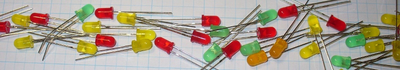
You can find LEDs in many different colours, and also units with two or more LEDs in the one housing, example red, green and blue. Some LEDs also create light in non-visible wavelengths, such as infra-red – these are used in remote-control applications and night-vision equipment. However if you are reading this, you would know by now where to find LEDs.

Well that wraps up my introduction to diodes. As always, thank you for reading and I look forward to your comments and so on. Please subscribe using one of the methods at the top-right of this web page to receive updates on new posts. Or join our new Google Group.

Otherwise, have fun and make something!

:)

Some information for this post came from various books by Forrest Mims III; ”All-new Electronics Self-Teaching Guide” by Harry Kybett and Earl Boysen; and data sheets by Fairchild, NXPON Semiconductor and Vishay; images of bridge rectifiers from Farnell Australia, LED and schottky diode symbols from electricalwhat.com.


  • Newsletter

    Sign up for the PlanetArduino Newsletter, which delivers the most popular articles via e-mail to your inbox every week. Just fill in the information below and submit.

  • Like Us on Facebook