Posts | Comments

Planet Arduino

Archive for the ‘NXP’ Category

Aug
13

Tutorial – Arduino and PCF8563 real time clock IC

arduino, clock, i2c, IC, NXP, PCF8563, real, Real-time clock, RTC, time, tronixstuff, tutorial Comments Off on Tutorial – Arduino and PCF8563 real time clock IC 

Use the NXP PCF8563 real-time clock IC with Arduino in chapter fifty-four of our Arduino Tutorials. The first chapter is here, the complete series is detailed here.

Updated 20/08/2013

Introduction

Recently a few people have been asking about the PCF8563 real-time clock IC from NXP – so this is a tutorial on how to use it for time, date, alarm clock and square-wave generation purposes.

The PCF8563 is another inexpensive RTC that can be used with an Arduino or other platforms due to the wide operating voltage (1 to 5.5V DC), I2C interface, and very low power consumption (when powered by a backup battery it only draws 0.25 μA). If you aren’t up to speed on the I2C interface, please review the I2C tutorials before moving forward. And please download the data sheet (.pdf).

The PCF8563 is available in various chip packages, for the curious we’re using the TSSOP8 version mounted on a breakout board:

PCF8563_SMD

Don’t panic – you can also get it in a breadboard-friendly DIP (through-hole) package as well, and also on a pre-built module from the usual suspects.

Demonstration Circuit

If you have a pre-made module, you can skip to the next section. However if you’re making up the circuit yourself, you will need:

  • One 32.768 kHz crystal
  • Two 1N4148 diodes*
  • One 3V coin cell (with holder)*
  • Two 10kΩ resistors
  • One 0.1 uF capacitor

And here’s the schematic:

PCF8563

* You can skip the diodes and battery if you don’t want a backup power supply when the main power is turned off or removed. Pin 3 is for the interrupt output (we’ll consider that later) and pin 7 is for the square-wave oscillator output.

Communicating with the PCF8563

Now to get down into the land of I2C once more. When looking through the data sheet NXP mentions two bus addresses, which have the same 7-bits finished with either a 1 for read or 0 for write. However you can just bitshift it over one bit as we don’t need the R/W bit – which gives you a bus address of 0×51.

Next you need to know which registers store the time and date – check the register map (table 4) on page 7 of the data sheet:

PCF8563 time date registers

 There will be a few other registers of interest, but we’ll return to those later. For now, note that the time and date start from 0×02. And one more thing – data is stored in the BCD (binary-coded- decimal) format. But don’t panic, we have a couple of functions to convert numbers between BCD and decimal.

Writing the time and date is a simple matter of collating the seconds, minutes, hours, day of week, day of month, month and year into bytes, converting to BCD then sending them to the PCF8563 with seven Wire.write() functions. Reading the data is also easy, just set the pointer to 0×02 and request seven bytes of data – then run them through a BCD to decimal conversion. With a catch.

And that catch is the need to sort out unwanted bits. Revisit table 4 in the data sheet – if you see an x that’s an unused bit. If any of them are a 1 they will mess up the BCD-decimal conversion when reading the register, so they need to be eliminated just like a whack-a-mole. To do this, we perform an & (bitwise AND) operation on the returned byte and mask out the unwanted bits with a zero. How does that work?

Example – the byte for dayOfMonth is returned – we only need bits 5 to 0. So 6 and 7 are superfluous. If you use (dayOfMonth & B00111111) the & function will set bits 6 and 7 to zero, and leave the other bits as they were.

Now to put all that together in a demonstration sketch. It puts everything mentioned to work and simply sets the time to the PCF8563, and then returns it to the serial monitor. The data is kept in global variables declared at the start of the sketch, and the conversions between BCD and decimal are done “on the fly” in the functions used to send or retrieve data from the PCF8563. Read through the following sketch and see how it works for yourself:

// Example 54.1 - PCF8563 RTC write/read demonstration

#include "Wire.h"
#define PCF8563address 0x51

byte second, minute, hour, dayOfWeek, dayOfMonth, month, year;
String days[] = {"Sunday", "Monday", "Tuesday", "Wednesday", "Thursday", "Friday", "Saturday" };

byte bcdToDec(byte value)
{
  return ((value / 16) * 10 + value % 16);
}

byte decToBcd(byte value){
  return (value / 10 * 16 + value % 10);
}

void setPCF8563()
// this sets the time and date to the PCF8563
{
  Wire.beginTransmission(PCF8563address);
  Wire.write(0x02);
  Wire.write(decToBcd(second));  
  Wire.write(decToBcd(minute));
  Wire.write(decToBcd(hour));     
  Wire.write(decToBcd(dayOfMonth));
  Wire.write(decToBcd(dayOfWeek));  
  Wire.write(decToBcd(month));
  Wire.write(decToBcd(year));
  Wire.endTransmission();
}

void readPCF8563()
// this gets the time and date from the PCF8563
{
  Wire.beginTransmission(PCF8563address);
  Wire.write(0x02);
  Wire.endTransmission();
  Wire.requestFrom(PCF8563address, 7);
  second     = bcdToDec(Wire.read() & B01111111); // remove VL error bit
  minute     = bcdToDec(Wire.read() & B01111111); // remove unwanted bits from MSB
  hour       = bcdToDec(Wire.read() & B00111111); 
  dayOfMonth = bcdToDec(Wire.read() & B00111111);
  dayOfWeek  = bcdToDec(Wire.read() & B00000111);  
  month      = bcdToDec(Wire.read() & B00011111);  // remove century bit, 1999 is over
  year       = bcdToDec(Wire.read());
}

void setup()
{
  Wire.begin();
  Serial.begin(9600);
  // change the following to set your initial time
  second = 0;
  minute = 28;
  hour = 9;
  dayOfWeek = 2;
  dayOfMonth = 13;
  month = 8;
  year = 13;
  // comment out the next line and upload again to set and keep the time from resetting every reset
  setPCF8563();
}

void loop()
{
  readPCF8563();
  Serial.print(days[dayOfWeek]); 
  Serial.print(" ");  
  Serial.print(dayOfMonth, DEC);
  Serial.print("/");
  Serial.print(month, DEC);
  Serial.print("/20");
  Serial.print(year, DEC);
  Serial.print(" - ");
  Serial.print(hour, DEC);
  Serial.print(":");
  if (minute < 10)
  {
    Serial.print("0");
  }
  Serial.print(minute, DEC);
  Serial.print(":");  
  if (second < 10)
  {
    Serial.print("0");
  }  
  Serial.println(second, DEC);  
  delay(1000);
}

And a quick video of this in operation:

If all you need to do is write and read the time with the PCF8563, you’re ready to go. However there’s a few more features of this unassuming little part which you might find useful, so at least keep reading…

Square-wave output

As with any clock or RTC IC, an oscillator is involved, and as mentioned earlier you can take this from pin 7 of the PCF8563. However – it’s an open-drain output – which means current flows from the supply voltage into pin 7. For example if you want to blink an LED, connect a 560Ω resistor between 5V and the anode of the LED, then connect the cathode to pin 7 of the PCF8563.

The frequency is controlled from the register at 0x0D. Simply write one of the following values for the respective frequencies:

  • 10000000 for 32.768 kHz;
  • 10000001 for 1.024 kHz;
  • 10000010 for 32 kHz;
  • 10000011 for 1 Hz;
  • 0 turns the output off and sets it to high impedance.

The following is a quick demonstration sketch which runs through the options:

// Example 54.2 - PCF8563 square-wave generator (signal from pin 7)

#include "Wire.h"
#define PCF8563address 0x51

void PCF8563oscOFF()
// turns off oscillator
{
  Wire.beginTransmission(PCF8563address);
  Wire.write(0x0D);
  Wire.write(0);
  Wire.endTransmission();
}

void PCF8563osc1Hz()
// sets oscillator to 1 Hz
{
  Wire.beginTransmission(PCF8563address);
  Wire.write(0x0D);
  Wire.write(B10000011);
  Wire.endTransmission();
}

void PCF8563osc32Hz()
// sets oscillator to 32 kHz
{
  Wire.beginTransmission(PCF8563address);
  Wire.write(0x0D);
  Wire.write(B10000010);
  Wire.endTransmission();
}

void PCF8563osc1024kHz()
// sets oscillator to 1.024 kHz
{
  Wire.beginTransmission(PCF8563address);
  Wire.write(0x0D);
  Wire.write(B10000001);
  Wire.endTransmission();
}

void PCF8563osc32768kHz()
// sets oscillator to 32.768 kHz
{
  Wire.beginTransmission(PCF8563address);
  Wire.write(0x0D);
  Wire.write(B10000000);
  Wire.endTransmission();
}

void setup()
{
  Wire.begin();
}

void loop()
{
  PCF8563osc1Hz();
  delay(2000);
  PCF8563osc32Hz();
  delay(2000);
  PCF8563osc1024kHz();
  delay(2000);
  PCF8563osc32768kHz();
  delay(2000);
  PCF8563oscOFF();
  delay(2000);
}

And the resulting waveforms from slowest to highest frequency. Note the sample was measured from a point between the LED and resistor, so the oscillations don’t vary between the supply voltage and zero:

PCF8563_1Hz

PCF8563_32Hz

PCF8563_1024Hz

PCF8563_32768Hz

Self-awareness of clock accuracy

The PCF8563 monitors the oscillator and supply voltage, and if the oscillator stops or the voltage drops below a certain point – the first bit of the seconds register (called the VL bit) is set to 1. Thus your sketch can tell you if there’s a chance of the time not being accurate by reading this bit. The default value is 1 on power-up, so you need to set it back to zero after setting the time in your sketch – which is done when you write seconds using the code in our example sketches. Then from that point it can be monitored by reading the seconds register, isolating the bit and returning the value.

Examine the function checkVLerror() in the following example sketch. It reads the seconds byte, isolates the VL bit, then turns on D13 (the onboard LED) if there’s a problem. The only way to restore the error bit to “OK” is to re-set the time:

// Example 54.3 - PCF8563 RTC write/read demonstration with error-checking

#include "Wire.h"
#define PCF8563address 0x51

byte second, minute, hour, dayOfWeek, dayOfMonth, month, year;
String days[] = {"Sunday", "Monday", "Tuesday", "Wednesday", "Thursday", "Friday", "Saturday" };

byte bcdToDec(byte value)
{
  return ((value / 16) * 10 + value % 16);
}

byte decToBcd(byte value){
  return (value / 10 * 16 + value % 10);
}

void setPCF8563()
// this sets the time and date to the PCF8563
{
  Wire.beginTransmission(PCF8563address);
  Wire.write(0x02);
  Wire.write(decToBcd(second));  
  Wire.write(decToBcd(minute));
  Wire.write(decToBcd(hour));     
  Wire.write(decToBcd(dayOfMonth));
  Wire.write(decToBcd(dayOfWeek));  
  Wire.write(decToBcd(month));
  Wire.write(decToBcd(year));
  Wire.endTransmission();
}

void readPCF8563()
// this gets the time and date from the PCF8563
{
  Wire.beginTransmission(PCF8563address);
  Wire.write(0x02);
  Wire.endTransmission();
  Wire.requestFrom(PCF8563address, 7);
  second     = bcdToDec(Wire.read() & B01111111); // remove VL error bit
  minute     = bcdToDec(Wire.read() & B01111111); // remove unwanted bits from MSB
  hour       = bcdToDec(Wire.read() & B00111111); 
  dayOfMonth = bcdToDec(Wire.read() & B00111111);
  dayOfWeek  = bcdToDec(Wire.read() & B00000111);  
  month      = bcdToDec(Wire.read() & B00011111);  // remove century bit, 1999 is over
  year       = bcdToDec(Wire.read());
}

void checkVLerror()
// this checks the VL bit in the seconds register
// and turns on D13 if there's a possible accuracy error
{
  byte test;
  Wire.beginTransmission(PCF8563address);
  Wire.write(0x02);
  Wire.endTransmission();
  Wire.requestFrom(PCF8563address, 1);
  test = Wire.read(); 
  test = test & B10000000;
  if (test == B10000000)
  {
    // error
    digitalWrite(13, HIGH);
    Serial.println("Uh-oh - possible accuracy error");
  } else 
  if (test != B10000000)
  {
    digitalWrite(13, LOW);
  }
}

void setup()
{
  Wire.begin();
  pinMode(13, OUTPUT);
  digitalWrite(13, HIGH);
  Serial.begin(9600);
  // change the following to set your inital time
  second = 0;
  minute = 42;
  hour = 11;
  dayOfWeek = 2;
  dayOfMonth = 13;
  month = 8;
  year = 13;
  // comment out the next line and upload again to set and keep the time from resetting every reset
  // setPCF8563();
}

void loop()
{
  readPCF8563();
  Serial.print(days[dayOfWeek]); 
  Serial.print(" ");  
  Serial.print(dayOfMonth, DEC);
  Serial.print("/");
  Serial.print(month, DEC);
  Serial.print("/20");
  Serial.print(year, DEC);
  Serial.print(" - ");
  Serial.print(hour, DEC);
  Serial.print(":");
  if (minute < 10)
  {
    Serial.print("0");
  }
  Serial.print(minute, DEC);
  Serial.print(":");  
  if (second < 10)
  {
    Serial.print("0");
  }  
  Serial.println(second, DEC);  
  checkVLerror();
  delay(1000);
}

And now for a demonstration of the error-checking at work. We have the PCF8563 happily returning the data to the serial monitor. Then the power is removed and restored. You see D13 on the Arduino-compatible board turn on and then the error is displayed in the serial monitor:

This function may sound frivolous, however if you’re building a real product or serious project using the PCF8563, you can use this feature to add a level of professionalism and instil confidence in the end user.

Alarm Clock

You can use the PCF8563 as an alarm clock, that is be notified of a certain time, day and/or day of the week – at which point an action can take place. For example, trigger an interrupt or turn on a digital output pin for an external siren. Etcetera. Using the alarm in the sketch is quite similar to reading and writing the time, the data is stored in certain registers – as shown in the following table from page seven of the data sheet:

PCF8563 alarm registers

However there is a catch – the MSB (most significant bit, 7) in the registers above is used to determine whether that particular register plays a part in the alarm. For example, if you want your alarm to include hours and minutes, bit 7 needs to be set to 1 for the hour and minute alarm register. Don’t panic – you can easily set that bit by using a bitwise OR (“|”) and B10000000 to set the bit on with the matching data before writing it to the register.

Checking if the alarm has occurred can be done with two methods – software and hardware. Using software you check bit 3 of the register at 0×01 (the “AF” alarm flag bit). If it’s 1 – it’s alarm time! Then you can turn the alarm off by setting that bit to zero. Using hardware, first set bit 1 of register 0×01 to 1 – then whenever an alarm occurs, current can flow into pin 3 of the PCF8563. Yes - it’s an open-drain output – which means current flows from the supply voltage into pin 3. For example if you want to turn on an LED, connect a 560Ω resistor between 5V and the anode of the LED, then connect the cathode to pin 3 of the PCF8563. To turn off this current, you need to turn off the alarm flag bit as mentioned earlier.

Now let’s put all that into a demonstration sketch. It’s documented and if you’ve been following along it shouldn’t be difficult at all:

// Example 54.4 - PCF8563 alarm clock demonstration

#include "Wire.h"
#define PCF8563address 0x51

byte second, minute, hour, dayOfWeek, dayOfMonth, month, year;
byte alarmMinute, alarmHour, alarmDay, alarmDayOfWeek;
String days[] = {"Sunday", "Monday", "Tuesday", "Wednesday", "Thursday", "Friday", "Saturday" };

byte bcdToDec(byte value)
{
  return ((value / 16) * 10 + value % 16);
}

byte decToBcd(byte value){
  return (value / 10 * 16 + value % 10);
}

void setPCF8563alarm()
// this sets the alarm data to the PCF8563
{
  byte am, ah, ad, adow;
  am = decToBcd(alarmMinute);
  am = am | 100000000; // set minute enable bit to on
  ah = decToBcd(alarmHour);
  ah = ah | 100000000; // set hour enable bit to on
  ad = decToBcd(alarmDay);
  ad = ad | 100000000; // set day of week alarm enable bit on
  adow = decToBcd(alarmDayOfWeek);
  adow = ad | 100000000; // set day of week alarm enable bit on

  // write alarm data to PCF8563
  Wire.beginTransmission(PCF8563address);
  Wire.write(0x09);
  Wire.write(am);  
  Wire.write(ah);

  // optional day of month and day of week (0~6 Sunday - Saturday)
  /*
  Wire.write(ad);
  Wire.write(adow);  
  */
  Wire.endTransmission();

  // optional - turns on INT_ pin when alarm activated  
  // will turn off once you run void PCF8563alarmOff()
  Wire.beginTransmission(PCF8563address);
  Wire.write(0x01);
  Wire.write(B00000010);
  Wire.endTransmission();
}

void PCF8563alarmOff()
// turns off alarm enable bits and wipes alarm registers. 
{
  byte test;
  // first retrieve the value of control register 2
  Wire.beginTransmission(PCF8563address);
  Wire.write(0x01);
  Wire.endTransmission();
  Wire.requestFrom(PCF8563address, 1);
  test = Wire.read();

  // set bit 3 "alarm flag" to 0
  test = test - B00001000;

  // now write new control register 2  
  Wire.beginTransmission(PCF8563address);
  Wire.write(0x01);
  Wire.write(test);
  Wire.endTransmission();
}

void checkPCF8563alarm()
// checks if the alarm has been activated
{
  byte test;
  // get the contents from control register #2 and place in byte test;
  Wire.beginTransmission(PCF8563address);
  Wire.write(0x01);
  Wire.endTransmission();
  Wire.requestFrom(PCF8563address, 1);
  test = Wire.read();
  test = test & B00001000; // isolate the alarm flag bit
  if (test == B00001000) // alarm on?
  {
    // alarm! Do something to tell the user
    Serial.println("** alarm **");
    delay(2000);

    // turn off the alarm
    PCF8563alarmOff();
  }
}

void setPCF8563()
// this sets the time and date to the PCF8563
{
  Wire.beginTransmission(PCF8563address);
  Wire.write(0x02);
  Wire.write(decToBcd(second));  
  Wire.write(decToBcd(minute));
  Wire.write(decToBcd(hour));     
  Wire.write(decToBcd(dayOfMonth));
  Wire.write(decToBcd(dayOfWeek));  
  Wire.write(decToBcd(month));
  Wire.write(decToBcd(year));
  Wire.endTransmission();
}

void readPCF8563()
// this gets the time and date from the PCF8563
{
  Wire.beginTransmission(PCF8563address);
  Wire.write(0x02);
  Wire.endTransmission();
  Wire.requestFrom(PCF8563address, 7);
  second     = bcdToDec(Wire.read() & B01111111); // remove VL error bit
  minute     = bcdToDec(Wire.read() & B01111111); // remove unwanted bits from MSB
  hour       = bcdToDec(Wire.read() & B00111111); 
  dayOfMonth = bcdToDec(Wire.read() & B00111111);
  dayOfWeek  = bcdToDec(Wire.read() & B00000111);  
  month      = bcdToDec(Wire.read() & B00011111);  // remove century bit, 1999 is over
  year       = bcdToDec(Wire.read());
}

void setup()
{
  Wire.begin();
  Serial.begin(9600);
  // change the following to set your initial time
  second = 50;
  minute = 44;
  hour = 13;
  dayOfWeek = 1;
  dayOfMonth = 19;
  month = 8;
  year = 13;
  // comment out the next line and upload again to set and keep the time from resetting every reset
  setPCF8563();

  alarmMinute = 45;
  alarmHour = 13;
  // comment out the next line and upload again to set and keep the alarm from resetting every reset  
  setPCF8563alarm();
}

void loop()
{
  readPCF8563();
  Serial.print(days[dayOfWeek]); 
  Serial.print(" ");  
  Serial.print(dayOfMonth, DEC);
  Serial.print("/");
  Serial.print(month, DEC);
  Serial.print("/20");
  Serial.print(year, DEC);
  Serial.print(" - ");
  Serial.print(hour, DEC);
  Serial.print(":");
  if (minute < 10)
  {
    Serial.print("0");
  }
  Serial.print(minute, DEC);
  Serial.print(":");  
  if (second < 10)
  {
    Serial.print("0");
  }  
  Serial.println(second, DEC);  
  delay(1000);

  // alarm?
  checkPCF8563alarm();
}

This is the same as the example 54.1, however we’ve added the required functions to use the alarm. The required alarm data is stored in the global bytes:

byte alarmMinute, alarmHour, alarmDay, alarmDayOfWeek;

and is written to the PCF8563 using the function:

void setPCF8563alarm()

Note the use of bitwise OR (“|”) to add the enable bit 7 to the data before writing to the register. The interrupt pin is also set to activate at the end of this function, however you can remove that part of the code if unnecessary. We also demonstrate checking the alarm status via software using the function:

void checkPCF8563alarm()

which simply reads the AF bit in the register at 0×01 and let’s us know if the alarm has occurred via the Serial Monitor. In this function you can add code to take action for your required needs. It also calls the function:

void PCF8563alarmOff()

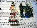
which retrieves the contents of the register at 0×01, sets the AF bit to zero and writes it back. We do this to preserve the status of the other bits in that register. For the curious and non-believers you can see this sketch in action through the following video, first the software and then the hardware interrupt pin method (an LED comes on at the alarm time and is then turned off:

 Conclusion

Hopefully you found this tutorial useful and now have the confidence to use the PCF8563 in your own projects. Furthermore I hope you learned something about the I2C bus and can have satisfaction in that you didn’t take the lazy option of using the library. People often say to me “Oh, there’s a library for that”, however if you used every library – you’d never learn how to interface things for yourself. One day there might not be a library! And then where would you be? So learning the hard way is better for you in the long run. If you have any questions leave a comment below, or ask privately via the contact page.

And if you enjoy my tutorials, or want to introduce someone else to the interesting world of Arduino – check out my book (now in a second printing) “Arduino Workshop” from No Starch Press.

In the meanwhile have fun and keep checking into tronixstuff.com. Why not follow things on twitterGoogle+, subscribe  for email updates or RSS using the links on the right-hand column? And join our friendly Google Group – dedicated to the projects and related items on this website. Sign up – it’s free, helpful to each other –  and we can all learn something.

The post Tutorial – Arduino and PCF8563 real time clock IC appeared first on tronixstuff.

Learn how to use the NXP PCF 8591 8-bit A/D and D/A IC with Arduino in chapter fifty-two of my Arduino Tutorials. The first chapter is here, the complete series is detailed here.

Updated 17/06/2013

Introduction

Have you ever wanted more analogue input pins on your Arduino project, but not wanted to fork out for a Mega? Or would you like to generate analogue signals? Then check out the subject of our tutorial – the NXP PCF8591 IC. It solves both these problems as it has a single DAC (digital to analogue) converter as well as four ADCs (analogue to digital converters) – all accessible via the I2C bus. If the I2C bus is new to you, please familiarise yourself with the readings here before moving forward.

The PCF8591 is available in DIP form, which makes it easy to experiment with:

pcf8591

You can get them from the usual retailers. Before moving on, download the data sheet. The PCF8591 can operate on both 5V and 3.3V so if you’re using an Arduino Due, Raspberry Pi or other 3.3 V development board you’re fine. Now we’ll first explain the DAC, then the ADCs.

Using the DAC (digital-to-analogue converter)

The DAC on the PCF8591 has a resolution of 8-bits – so it can generate a theoretical signal of between zero volts and the reference voltage (Vref) in 255 steps. For demonstration purposes we’ll use a Vref of 5V, and you can use a lower Vref such as 3.3V or whatever you wish the maximum value to be … however it must be less than the supply voltage. Note that when there is a load on the analogue output (a real-world situation), the maximum output voltage will drop – the data sheet (which you downloaded) shows a 10% drop for a 10kΩ load. Now for our demonstration circuit:

pcf8591basic_schem

Note the use of 10kΩ pull-up resistors on the I2C bus, and the 10μF capacitor between 5V and GND. The I2C bus address is set by a combination of pins A0~A2, and with them all to GND the address is 0×90. The analogue output can be taken from pin 15 (and there’s a seperate analogue GND on pin 13. Also, connect pin 13 to GND, and circuit GND to Arduino GND.

To control the DAC we need to send two bytes of data. The first is the control byte, which simply activates the DAC and is 1000000 (or 0×40) and the next byte is the value between 0 and 255 (the output level). This is demonstrated in the following sketch:

// Example 52.1 PCF8591 DAC demo
// http://tronixstuff.com/tutorials Chapter 52
// John Boxall June 2013
#include "Wire.h"
#define PCF8591 (0x90 >> 1) // I2C bus address
void setup()
{
 Wire.begin();
}
void loop()
{
 for (int i=0; i<256; i++)
 {
 Wire.beginTransmission(PCF8591); // wake up PCF8591
 Wire.write(0x40); // control byte - turn on DAC (binary 1000000)
 Wire.write(i); // value to send to DAC
 Wire.endTransmission(); // end tranmission
 }

 for (int i=255; i>=0; --i)
 {
 Wire.beginTransmission(PCF8591); // wake up PCF8591
 Wire.write(0x40); // control byte - turn on DAC (binary 1000000)
 Wire.write(i); // value to send to DAC
 Wire.endTransmission(); // end tranmission
 }
}

Did you notice the bit shift of the bus address in the #define statement? Arduino sends 7-bit addresses but the PCF8591 wants an 8-bit, so we shift the byte over by one bit. 

The results of the sketch are shown below, we’ve connected the Vref to 5V and the oscilloscope probe and GND to the analogue output and GND respectively:

triangle

If you like curves you can generate sine waves with the sketch below. It uses a lookup table in an array which contains the necessary pre-calculated data points:

// Example 52.2 PCF8591 DAC demo - sine wave
// http://tronixstuff.com/tutorials Chapter 52
// John Boxall June 2013

#include "Wire.h"
#define PCF8591 (0x90 >> 1) // I2C bus address

uint8_t sine_wave[256] = {
 0x80, 0x83, 0x86, 0x89, 0x8C, 0x90, 0x93, 0x96,
 0x99, 0x9C, 0x9F, 0xA2, 0xA5, 0xA8, 0xAB, 0xAE,
 0xB1, 0xB3, 0xB6, 0xB9, 0xBC, 0xBF, 0xC1, 0xC4,
 0xC7, 0xC9, 0xCC, 0xCE, 0xD1, 0xD3, 0xD5, 0xD8,
 0xDA, 0xDC, 0xDE, 0xE0, 0xE2, 0xE4, 0xE6, 0xE8,
 0xEA, 0xEB, 0xED, 0xEF, 0xF0, 0xF1, 0xF3, 0xF4,
 0xF5, 0xF6, 0xF8, 0xF9, 0xFA, 0xFA, 0xFB, 0xFC,
 0xFD, 0xFD, 0xFE, 0xFE, 0xFE, 0xFF, 0xFF, 0xFF,
 0xFF, 0xFF, 0xFF, 0xFF, 0xFE, 0xFE, 0xFE, 0xFD,
 0xFD, 0xFC, 0xFB, 0xFA, 0xFA, 0xF9, 0xF8, 0xF6,
 0xF5, 0xF4, 0xF3, 0xF1, 0xF0, 0xEF, 0xED, 0xEB,
 0xEA, 0xE8, 0xE6, 0xE4, 0xE2, 0xE0, 0xDE, 0xDC,
 0xDA, 0xD8, 0xD5, 0xD3, 0xD1, 0xCE, 0xCC, 0xC9,
 0xC7, 0xC4, 0xC1, 0xBF, 0xBC, 0xB9, 0xB6, 0xB3,
 0xB1, 0xAE, 0xAB, 0xA8, 0xA5, 0xA2, 0x9F, 0x9C,
 0x99, 0x96, 0x93, 0x90, 0x8C, 0x89, 0x86, 0x83,
 0x80, 0x7D, 0x7A, 0x77, 0x74, 0x70, 0x6D, 0x6A,
 0x67, 0x64, 0x61, 0x5E, 0x5B, 0x58, 0x55, 0x52,
 0x4F, 0x4D, 0x4A, 0x47, 0x44, 0x41, 0x3F, 0x3C,
 0x39, 0x37, 0x34, 0x32, 0x2F, 0x2D, 0x2B, 0x28,
 0x26, 0x24, 0x22, 0x20, 0x1E, 0x1C, 0x1A, 0x18,
 0x16, 0x15, 0x13, 0x11, 0x10, 0x0F, 0x0D, 0x0C,
 0x0B, 0x0A, 0x08, 0x07, 0x06, 0x06, 0x05, 0x04,
 0x03, 0x03, 0x02, 0x02, 0x02, 0x01, 0x01, 0x01,
 0x01, 0x01, 0x01, 0x01, 0x02, 0x02, 0x02, 0x03,
 0x03, 0x04, 0x05, 0x06, 0x06, 0x07, 0x08, 0x0A,
 0x0B, 0x0C, 0x0D, 0x0F, 0x10, 0x11, 0x13, 0x15,
 0x16, 0x18, 0x1A, 0x1C, 0x1E, 0x20, 0x22, 0x24,
 0x26, 0x28, 0x2B, 0x2D, 0x2F, 0x32, 0x34, 0x37,
 0x39, 0x3C, 0x3F, 0x41, 0x44, 0x47, 0x4A, 0x4D,
 0x4F, 0x52, 0x55, 0x58, 0x5B, 0x5E, 0x61, 0x64,
 0x67, 0x6A, 0x6D, 0x70, 0x74, 0x77, 0x7A, 0x7D
};
void setup()
{
 Wire.begin();
}
void loop()
{
 for (int i=0; i<256; i++)
 {
 Wire.beginTransmission(PCF8591); // wake up PCF8591
 Wire.write(0x40); // control byte - turn on DAC (binary 1000000)
 Wire.write(sine_wave[i]); // value to send to DAC
 Wire.endTransmission(); // end tranmission
 }
}

And the results:

sine

For the following DSO image dump, we changed the Vref to 3.3V – note the change in the maxima on the sine wave:

sine3v3

Now you can experiment with the DAC to make sound effects, signals or control other analogue circuits.

Using the ADCs (analogue-to-digital converters)

If you’ve used the analogRead() function on your Arduino (way back in Chapter One) then you’re already familiar with an ADC. With out PCF8591 we can read a voltage between zero and the Vref and it will return a value of between zero and 255 which is directly proportional to zero and the Vref. For example, measuring 3.3V should return 168. The resolution (8-bit) of the ADC is lower than the onboard Arduino (10-bit) however the PCF8591 can do something the Arduino’s ADC cannot. But we’ll get to that in a moment.

First, to simply read the values of each ADC pin we send a control byte to tell the PCF8591 which ADC we want to read. For ADCs zero to three the control byte is 0×00, 0×01, ox02 and 0×03 respectively. Then we ask for two bytes of data back from the ADC, and store the second byte for use. Why two bytes? The PCF8591 returns the previously measured value first – then the current byte. (See Figure 8 in the data sheet). Finally, if you’re not using all the ADC pins, connect the unused ones to GND.

The following example sketch simply retrieves values from each ADC pin one at a time, then displays them in the serial monitor:

// Example 52.3 PCF8591 ADC demo
// http://tronixstuff.com/tutorials Chapter 52
// John Boxall June 2013
#include "Wire.h"
#define PCF8591 (0x90 >> 1) // I2C bus address
#define ADC0 0x00 // control bytes for reading individual ADCs
#define ADC1 0x01
#define ADC2 0x02
#define ADC3 0x03
byte value0, value1, value2, value3;
void setup()
{
 Wire.begin();
 Serial.begin(9600);
}
void loop()
{
 Wire.beginTransmission(PCF8591); // wake up PCF8591
 Wire.write(ADC0); // control byte - read ADC0
 Wire.endTransmission(); // end tranmission
 Wire.requestFrom(PCF8591, 2);
 value0=Wire.read();
 value0=Wire.read();
 Wire.beginTransmission(PCF8591); // wake up PCF8591
 Wire.write(ADC1); // control byte - read ADC1
 Wire.endTransmission(); // end tranmission
 Wire.requestFrom(PCF8591, 2);
 value1=Wire.read();
 value1=Wire.read();
 Wire.beginTransmission(PCF8591); // wake up PCF8591
 Wire.write(ADC2); // control byte - read ADC2
 Wire.endTransmission(); // end tranmission
 Wire.requestFrom(PCF8591, 2);
 value2=Wire.read();
 value2=Wire.read();
 Wire.beginTransmission(PCF8591); // wake up PCF8591
 Wire.write(ADC3); // control byte - read ADC3
 Wire.endTransmission(); // end tranmission
 Wire.requestFrom(PCF8591, 2);
 value3=Wire.read();
 value3=Wire.read();
 Serial.print(value0); Serial.print(" ");
 Serial.print(value1); Serial.print(" ");
 Serial.print(value2); Serial.print(" ");
 Serial.print(value3); Serial.print(" ");
 Serial.println();
}

Upon running the sketch you’ll be presented with the values of each ADC in the serial monitor. Although it was a simple demonstration to show you how to individually read each ADC, it is a cumbersome method of getting more than one byte at a time from a particular ADC.

To do this, change the control byte to request auto-increment, which is done by setting bit 2 of the control byte to 1. So to start from ADC0 we use a new control byte of binary 00000100 or hexadecimal 0×04. Then request five bytes of data (once again we ignore the first byte) which will cause the PCF8591 to return all values in one chain of bytes. This process is demonstrated in the following sketch:

// Example 52.4 PCF8591 ADC demo
// http://tronixstuff.com/tutorials Chapter 52
// John Boxall June 2013
#include "Wire.h"
#define PCF8591 (0x90 >> 1) // I2C bus address
byte value0, value1, value2, value3;
void setup()
{
 Wire.begin();
 Serial.begin(9600);
}
void loop()
{
 Wire.beginTransmission(PCF8591); // wake up PCF8591
 Wire.write(0x04); // control byte - read ADC0 then auto-increment
 Wire.endTransmission(); // end tranmission
 Wire.requestFrom(PCF8591, 5);
 value0=Wire.read();
 value0=Wire.read();
 value1=Wire.read();
 value2=Wire.read();
 value3=Wire.read();
 Serial.print(value0); Serial.print(" ");
 Serial.print(value1); Serial.print(" ");
 Serial.print(value2); Serial.print(" ");
 Serial.print(value3); Serial.print(" ");
 Serial.println();
}

Previously we mentioned that the PCF8591 can do something that the Arduino’s ADC cannot, and this is offer a differential ADC. As opposed to the Arduino’s single-ended (i.e. it returns the difference between the positive signal voltage and GND, the differential ADC accepts two signals (that don’t necessarily have to be referenced to ground), and returns the difference between the two signals. This can be convenient for measuring small changes in voltages for load cells and so on.

Setting up the PCF8591 for differential ADC is a simple matter of changing the control byte. If you turn to page seven of the data sheet, then consider the different types of analogue input programming. Previously we used mode ’00′ for four inputs, however you can select the others which are clearly illustrated, for example:

adcmodes

So to set the control byte for two differential inputs, use binary 00110000 or 0×30. Then it’s a simple matter of requesting the bytes of data and working with them. As you can see there’s also combination single/differential and a complex three-differential input. However we’ll leave them for the time being.

Conclusion

Hopefully you found this of interest, whether adding a DAC to your experiments or learning a bit more about ADCs. We’ll have some more analogue to digital articles coming up soon, so stay tuned. And if you enjoy my tutorials, or want to introduce someone else to the interesting world of Arduino – check out my new book “Arduino Workshop” from No Starch Press.

LEDborder

In the meanwhile have fun and keep checking into tronixstuff.com. Why not follow things on twitterGoogle+, subscribe  for email updates or RSS using the links on the right-hand column? And join our friendly Google Group – dedicated to the projects and related items on this website. Sign up – it’s free, helpful to each other –  and we can all learn something.

The post Tutorial – Arduino and PCF8591 ADC DAC IC appeared first on tronixstuff.

Learn how to use the NXP PCF 8591 8-bit A/D and D/A IC with Arduino in chapter fifty-two of my Arduino Tutorials. The first chapter is here, the complete series is detailed here.

Updated 17/06/2013

Introduction

Have you ever wanted more analogue input pins on your Arduino project, but not wanted to fork out for a Mega? Or would you like to generate analogue signals? Then check out the subject of our tutorial – the NXP PCF8591 IC. It solves both these problems as it has a single DAC (digital to analogue) converter as well as four ADCs (analogue to digital converters) – all accessible via the I2C bus. If the I2C bus is new to you, please familiarise yourself with the readings here before moving forward.

The PCF8591 is available in DIP form, which makes it easy to experiment with:

pcf8591

You can get them from the usual retailers. Before moving on, download the data sheet. The PCF8591 can operate on both 5V and 3.3V so if you’re using an Arduino Due, Raspberry Pi or other 3.3 V development board you’re fine. Now we’ll first explain the DAC, then the ADCs.

Using the DAC (digital-to-analogue converter)

The DAC on the PCF8591 has a resolution of 8-bits – so it can generate a theoretical signal of between zero volts and the reference voltage (Vref) in 255 steps. For demonstration purposes we’ll use a Vref of 5V, and you can use a lower Vref such as 3.3V or whatever you wish the maximum value to be … however it must be less than the supply voltage. Note that when there is a load on the analogue output (a real-world situation), the maximum output voltage will drop – the data sheet (which you downloaded) shows a 10% drop for a 10kΩ load. Now for our demonstration circuit:

pcf8591basic_schem

Note the use of 10kΩ pull-up resistors on the I2C bus, and the 10μF capacitor between 5V and GND. The I2C bus address is set by a combination of pins A0~A2, and with them all to GND the address is 0×90. The analogue output can be taken from pin 15 (and there’s a seperate analogue GND on pin 13. Also, connect pin 13 to GND, and circuit GND to Arduino GND.

To control the DAC we need to send two bytes of data. The first is the control byte, which simply activates the DAC and is 1000000 (or 0×40) and the next byte is the value between 0 and 255 (the output level). This is demonstrated in the following sketch (download):

// Example 52.1 PCF8591 DAC demo
// http://tronixstuff.com/tutorials Chapter 52
// John Boxall June 2013
#include "Wire.h"
#define PCF8591 (0x90 >> 1) // I2C bus address
void setup()
{
 Wire.begin();
}
void loop()
{ 
 for (int i=0; i<256; i++)
 {
 Wire.beginTransmission(PCF8591); // wake up PCF8591
 Wire.write(0x40); // control byte - turn on DAC (binary 1000000)
 Wire.write(i); // value to send to DAC
 Wire.endTransmission(); // end tranmission
 }

 for (int i=255; i>=0; --i)
 {
 Wire.beginTransmission(PCF8591); // wake up PCF8591
 Wire.write(0x40); // control byte - turn on DAC (binary 1000000)
 Wire.write(i); // value to send to DAC
 Wire.endTransmission(); // end tranmission
 }
}

Did you notice the bit shift of the bus address in the #define statement? Arduino sends 7-bit addresses but the PCF8591 wants an 8-bit, so we shift the byte over by one bit. 

The results of the sketch are shown below, we’ve connected the Vref to 5V and the oscilloscope probe and GND to the analogue output and GND respectively (click image to enlarge):

triangle

If you like curves you can generate sine waves with the sketch below. It uses a lookup table in an array which contains the necessary pre-calculated data points (download):

// Example 52.2 PCF8591 DAC demo - sine wave
// http://tronixstuff.com/tutorials Chapter 52
// John Boxall June 2013
#include "Wire.h"
#define PCF8591 (0x90 >> 1) // I2C bus address
uint8_t sine_wave[256] = {
 0x80, 0x83, 0x86, 0x89, 0x8C, 0x90, 0x93, 0x96,
 0x99, 0x9C, 0x9F, 0xA2, 0xA5, 0xA8, 0xAB, 0xAE,
 0xB1, 0xB3, 0xB6, 0xB9, 0xBC, 0xBF, 0xC1, 0xC4,
 0xC7, 0xC9, 0xCC, 0xCE, 0xD1, 0xD3, 0xD5, 0xD8,
 0xDA, 0xDC, 0xDE, 0xE0, 0xE2, 0xE4, 0xE6, 0xE8,
 0xEA, 0xEB, 0xED, 0xEF, 0xF0, 0xF1, 0xF3, 0xF4,
 0xF5, 0xF6, 0xF8, 0xF9, 0xFA, 0xFA, 0xFB, 0xFC,
 0xFD, 0xFD, 0xFE, 0xFE, 0xFE, 0xFF, 0xFF, 0xFF,
 0xFF, 0xFF, 0xFF, 0xFF, 0xFE, 0xFE, 0xFE, 0xFD,
 0xFD, 0xFC, 0xFB, 0xFA, 0xFA, 0xF9, 0xF8, 0xF6,
 0xF5, 0xF4, 0xF3, 0xF1, 0xF0, 0xEF, 0xED, 0xEB,
 0xEA, 0xE8, 0xE6, 0xE4, 0xE2, 0xE0, 0xDE, 0xDC,
 0xDA, 0xD8, 0xD5, 0xD3, 0xD1, 0xCE, 0xCC, 0xC9,
 0xC7, 0xC4, 0xC1, 0xBF, 0xBC, 0xB9, 0xB6, 0xB3,
 0xB1, 0xAE, 0xAB, 0xA8, 0xA5, 0xA2, 0x9F, 0x9C,
 0x99, 0x96, 0x93, 0x90, 0x8C, 0x89, 0x86, 0x83,
 0x80, 0x7D, 0x7A, 0x77, 0x74, 0x70, 0x6D, 0x6A,
 0x67, 0x64, 0x61, 0x5E, 0x5B, 0x58, 0x55, 0x52,
 0x4F, 0x4D, 0x4A, 0x47, 0x44, 0x41, 0x3F, 0x3C,
 0x39, 0x37, 0x34, 0x32, 0x2F, 0x2D, 0x2B, 0x28,
 0x26, 0x24, 0x22, 0x20, 0x1E, 0x1C, 0x1A, 0x18,
 0x16, 0x15, 0x13, 0x11, 0x10, 0x0F, 0x0D, 0x0C,
 0x0B, 0x0A, 0x08, 0x07, 0x06, 0x06, 0x05, 0x04,
 0x03, 0x03, 0x02, 0x02, 0x02, 0x01, 0x01, 0x01,
 0x01, 0x01, 0x01, 0x01, 0x02, 0x02, 0x02, 0x03,
 0x03, 0x04, 0x05, 0x06, 0x06, 0x07, 0x08, 0x0A,
 0x0B, 0x0C, 0x0D, 0x0F, 0x10, 0x11, 0x13, 0x15,
 0x16, 0x18, 0x1A, 0x1C, 0x1E, 0x20, 0x22, 0x24,
 0x26, 0x28, 0x2B, 0x2D, 0x2F, 0x32, 0x34, 0x37,
 0x39, 0x3C, 0x3F, 0x41, 0x44, 0x47, 0x4A, 0x4D,
 0x4F, 0x52, 0x55, 0x58, 0x5B, 0x5E, 0x61, 0x64,
 0x67, 0x6A, 0x6D, 0x70, 0x74, 0x77, 0x7A, 0x7D
};
void setup()
{
 Wire.begin();
}
void loop()
{ 
 for (int i=0; i<256; i++)
 {
 Wire.beginTransmission(PCF8591); // wake up PCF8591
 Wire.write(0x40); // control byte - turn on DAC (binary 1000000)
 Wire.write(sine_wave[i]); // value to send to DAC
 Wire.endTransmission(); // end tranmission
 }
}

And the results (click image to enlarge):

sine

For the following DSO image dump, we changed the Vref to 3.3V – note the change in the maxima on the sine wave:

sine3v3

Now you can experiment with the DAC to make sound effects, signals or control other analogue circuits.

Using the ADCs (analogue-to-digital converters)

If you’ve used the analogRead() function on your Arduino (way back in Chapter One) then you’re already familiar with an ADC. With out PCF8591 we can read a voltage between zero and the Vref and it will return a value of between zero and 255 which is directly proportional to zero and the Vref. For example, measuring 3.3V should return 168. The resolution (8-bit) of the ADC is lower than the onboard Arduino (10-bit) however the PCF8591 can do something the Arduino’s ADC cannot. But we’ll get to that in a moment.

First, to simply read the values of each ADC pin we send a control byte to tell the PCF8591 which ADC we want to read. For ADCs zero to three the control byte is 0×00, 0×01, ox02 and 0×03 respectively. Then we ask for two bytes of data back from the ADC, and store the second byte for use. Why two bytes? The PCF8591 returns the previously measured value first – then the current byte. (See Figure 8 in the data sheet). Finally, if you’re not using all the ADC pins, connect the unused ones to GND.

The following example sketch simply retrieves values from each ADC pin one at a time, then displays them in the serial monitor (download):

// Example 52.3 PCF8591 ADC demo 
// http://tronixstuff.com/tutorials Chapter 52
// John Boxall June 2013
#include "Wire.h"
#define PCF8591 (0x90 >> 1) // I2C bus address
#define ADC0 0x00 // control bytes for reading individual ADCs
#define ADC1 0x01
#define ADC2 0x02
#define ADC3 0x03
byte value0, value1, value2, value3;
void setup()
{
 Wire.begin();
 Serial.begin(9600);
}
void loop()
{ 
 Wire.beginTransmission(PCF8591); // wake up PCF8591
 Wire.write(ADC0); // control byte - read ADC0
 Wire.endTransmission(); // end tranmission
 Wire.requestFrom(PCF8591, 2);
 value0=Wire.read();
 value0=Wire.read();
 Wire.beginTransmission(PCF8591); // wake up PCF8591
 Wire.write(ADC1); // control byte - read ADC1
 Wire.endTransmission(); // end tranmission
 Wire.requestFrom(PCF8591, 2);
 value1=Wire.read();
 value1=Wire.read();
 Wire.beginTransmission(PCF8591); // wake up PCF8591
 Wire.write(ADC2); // control byte - read ADC2
 Wire.endTransmission(); // end tranmission
 Wire.requestFrom(PCF8591, 2);
 value2=Wire.read();
 value2=Wire.read();
 Wire.beginTransmission(PCF8591); // wake up PCF8591
 Wire.write(ADC3); // control byte - read ADC3
 Wire.endTransmission(); // end tranmission
 Wire.requestFrom(PCF8591, 2);
 value3=Wire.read();
 value3=Wire.read();
 Serial.print(value0); Serial.print(" ");
 Serial.print(value1); Serial.print(" ");
 Serial.print(value2); Serial.print(" ");
 Serial.print(value3); Serial.print(" "); 
 Serial.println();
}

Upon running the sketch you’ll be presented with the values of each ADC in the serial monitor. Although it was a simple demonstration to show you how to individually read each ADC, it is a cumbersome method of getting more than one byte at a time from a particular ADC.

To do this, change the control byte to request auto-increment, which is done by setting bit 2 of the control byte to 1. So to start from ADC0 we use a new control byte of binary 00000100 or hexadecimal 0×04. Then request five bytes of data (once again we ignore the first byte) which will cause the PCF8591 to return all values in one chain of bytes. This process is demonstrated in the following sketch (download):

// Example 52.4 PCF8591 ADC demo 
// http://tronixstuff.com/tutorials Chapter 52
// John Boxall June 2013
#include "Wire.h"
#define PCF8591 (0x90 >> 1) // I2C bus address
byte value0, value1, value2, value3;
void setup()
{
 Wire.begin();
 Serial.begin(9600);
}
void loop()
{ 
 Wire.beginTransmission(PCF8591); // wake up PCF8591
 Wire.write(0x04); // control byte - read ADC0 then auto-increment
 Wire.endTransmission(); // end tranmission
 Wire.requestFrom(PCF8591, 5); 
 value0=Wire.read();
 value0=Wire.read(); 
 value1=Wire.read(); 
 value2=Wire.read(); 
 value3=Wire.read();
 Serial.print(value0); Serial.print(" ");
 Serial.print(value1); Serial.print(" ");
 Serial.print(value2); Serial.print(" ");
 Serial.print(value3); Serial.print(" "); 
 Serial.println();
}

Previously we mentioned that the PCF8591 can do something that the Arduino’s ADC cannot, and this is offer a differential ADC. As opposed to the Arduino’s single-ended (i.e. it returns the difference between the positive signal voltage and GND, the differential ADC accepts two signals (that don’t necessarily have to be referenced to ground), and returns the difference between the two signals. This can be convenient for measuring small changes in voltages for load cells and so on.

Setting up the PCF8591 for differential ADC is a simple matter of changing the control byte. If you turn to page seven of the data sheet, then consider the different types of analogue input programming. Previously we used mode ’00′ for four inputs, however you can select the others which are clearly illustrated, for example:

adcmodes

So to set the control byte for two differential inputs, use binary 00110000 or 0×30. Then it’s a simple matter of requesting the bytes of data and working with them. As you can see there’s also combination single/differential and a complex three-differential input. However we’ll leave them for the time being.

Conclusion

Hopefully you found this of interest, whether adding a DAC to your experiments or learning a bit more about ADCs. We’ll have some more analogue to digital articles coming up soon, so stay tuned. And if you enjoy my tutorials, or want to introduce someone else to the interesting world of Arduino – check out my new book “Arduino Workshop” from No Starch Press.

In the meanwhile have fun and keep checking into tronixstuff.com. Why not follow things on twitterGoogle+, subscribe  for email updates or RSS using the links on the right-hand column? And join our friendly Google Group – dedicated to the projects and related items on this website. Sign up – it’s free, helpful to each other –  and we can all learn something.


Hello readers

Today we are going to examine the 74HC238 decoder/demultiplexer IC. My reason for writing this was to examine another way to get more output pins when using an Arduino or compatible board. However you can use any combination of three logic lines to turn on or off eight mutually exclusive outputs. How? Let’s find out…

First of all, here is the IC:

It is also available in SO16, SSOP16,  TSSOP16 and DHVQFN16 packages. What? Here is a good list of various SMD packaging types. Although my sample is from NXP, a quick search shows it is also made by Texas Instruments and ST Microelectronics. Here is the NXP data sheet.

The pin layout is very simple, apart from +5V and ground, you have six pins that control the outputs, and eight output pins, however in reality you only need to control three from the microcontroller or other logic lines. Here is the pinout diagram:

To get the output pins high, you use a combination of levels on pins A0~A2 and possibly E3. If you leave E3 low, no outputs can be set to high. The input combination required for each output is described in this table from the data sheet (click to enlarge):

Notice that columns with an X can be set either high or low, but you must not leave them floating, so always connect or set an X to high or low. If you need to have active low outputs (that is, outputs are high instead of low), there is the 74HC138. So now to do this in real life! Here is a demonstration schematic to use the 74HC238 with an Arduino Duemilanove or 100% compatible board:


… and in real life:

And here is a demonstration video, using this arduino sketch: 74HC238Arduino.pdf

Question: In real life, in which country is the Hoff a popular singer?

As with most other ICs of this type, you can only source 25 milliamps of current from each output, so if you need more you will have to consider the use of a switching NPN transistor etc. Although only one output can be high at a time, if you scan them quick enough, you can create the illusion that all are on at once (as in the video). Apart from LEDs and other items, you could use this IC to control stepper motors or even create a safeworking environment on a model train layout.

To conclude, the 74HC238 offers one of several ways to control more things with less control pins. Ideal for mutually exclusive outputs, however if you needed more than one high at once, the 74HC595 shift register would be the better solution. (See here for a 74HC595 tutorial).

As always, avoid the risk of counterfeit ICs and get yours from a reputable distributor. Living in Australia, mine came from Little Bird Electronics.

Once again, thank you for reading and I look forward to your comments and so on. Furthermore, don’t be shy in pointing out errors or places that could use improvement. Please subscribe using one of the methods at the top-right of this web page to receive updates on new posts. Or join our new Google Group. High resolution photos are available on flickr.

Otherwise, have fun, be good to each other – and make something! :)

Hello readers!

Today we are going to examine the 74HC4066 quad bilateral switch IC. My reason for writing this comes from a comment left by a reader on chapter nine of the Arduino tutorial. They suggested using a 4066 IC to control the cathodes of the LED matrix instead of resistors and NPN transistors. This was a good suggestion, however the 4066 can only switch a current of 10mA per pin. Luckily the 74HC4066 can handle up to 25mA per switch – so we’ll look into this instead.

First of all, let’s say hello:

This is the 14-pin DIP package. It is also available in surface mount, and other newer package styles. Although we are looking at an example from NXP, according to my main component supplier (Farnell/Newark) this IC is also manufactured by Texas Instruments, ON Semi, ST Microelectronics and Fairchild.

So, what is a quad-bilateral switch? Four switches in one IC. Here is a diagram:

Imagine a simple normally-open push button. You press the button, and current can flow through the switch. Using the 74HC4066, when current is applied to the E pin, current can pass through from the matching Y pin to the Z pin. As you can see above, there are four of these switches in the IC. This is where the benefit of the IC comes to mind, normally one might use a 1k ohm resistor and an NPN switching transistor as an electronic switch, and I have done so myself. But when you need a few of them, it can be easier to start using these 74HC4066s as long as the current requirements are met.

With regards to the current the IC can switch, Is, the maximum is 25mA per switch. This is more than enough to run a typical LED, TTL logic gate, etc. The other interesting parameter is the turn-on and turn off times – at 6 volts it can turn on in around 10 nanoseconds and turn off at around 13 nanoseconds (so a rough calculation – say it takes 30 nanoseconds to switch on and then switch off, that’s 33.3 million times per seconds (33.3 MHz). All these parameters and more are available from the data sheet (pdf). Someone correct me if I’m wrong!

That’s enough theory – let’s put it to work now. Our first demonstration is quite simple – just switch on and off some LEDs via a 74HC595 shift register and an Arduino. We send a number (0, 1, 2, 4, 8 ) to the shift register, which stays off, then sets pins Q0, Q1, Q2, Q3 high in order, which in turn activate the switches 1~4 on the 74HC4066. The 74HC4066 sends a current to each LED connected to the switch outputs.

Here is the schematic:

Laid out on the breadboard:

And the ubiquitous video:

And here is the Arduino sketch: demo1.pdf. Well that was interesting. I know these simple demonstrations may be… well a little simple, but after taking the time to build them from scratch you get a better understanding of the part and how they work. Practice makes perfect and all that. Anyhow, let’s have a look at something much more interesting – a very basic (!) digital to analogue converter. Consider the circuit below:

The 74HC4066 switches creates a final voltage through the sum of various currents being switched into the final output. First of all, here is a video of the switches being turned on and off one at a time:

and the corresponding Arduino sketch:demo2.pdf. The next video shows the results of sending decimal numbers 0~15 to the shift register – in effect continually adding the outputs of the pins until all pins are on, then in reverse:

and the corresponding Ardiono sketch:demo3.pdf.

Well I hope you found this part review interesting, and helped you think of something new to make. In conclusion I would consider the 74HC4066 easier and quicker for end user to use in projects (less pins to solder, etc) however using it could cost more depending on the volume required. Furthermore, this would only apply if the current restrictions of the IC are met.

As always, thank you for reading and I look forward to your comments and so on. Furthermore, don’t be shy in pointing out errors or places that could use improvement. Please subscribe using one of the methods at the top-right of this web page to receive updates on new posts. Or join our new Google Group. High resolution photos are available on flickr.

Otherwise, have fun, be good to each other – and make something! :)

Notes: In writing this post, I used information from NXP, plus information and circuit inspiration from various books by Forrest Mims III.

Thank you!


  • Newsletter

    Sign up for the PlanetArduino Newsletter, which delivers the most popular articles via e-mail to your inbox every week. Just fill in the information below and submit.

  • Like Us on Facebook